

 Home
-
RF PCB
-
Rogers RO4725JXR Antenna RF PCB Double-Layer 0.78mm Substrates with Copper and Immersion Gold
Home
-
RF PCB
-
Rogers RO4725JXR Antenna RF PCB Double-Layer 0.78mm Substrates with Copper and Immersion Gold
Rogers RO4725JXR Antenna RF PCB Double-Layer 0.78mm Substrates with Copper and Immersion Gold
Printed Circuit Boards are custom-made products; the images and specifications provided are for reference only.
Brief Introduction
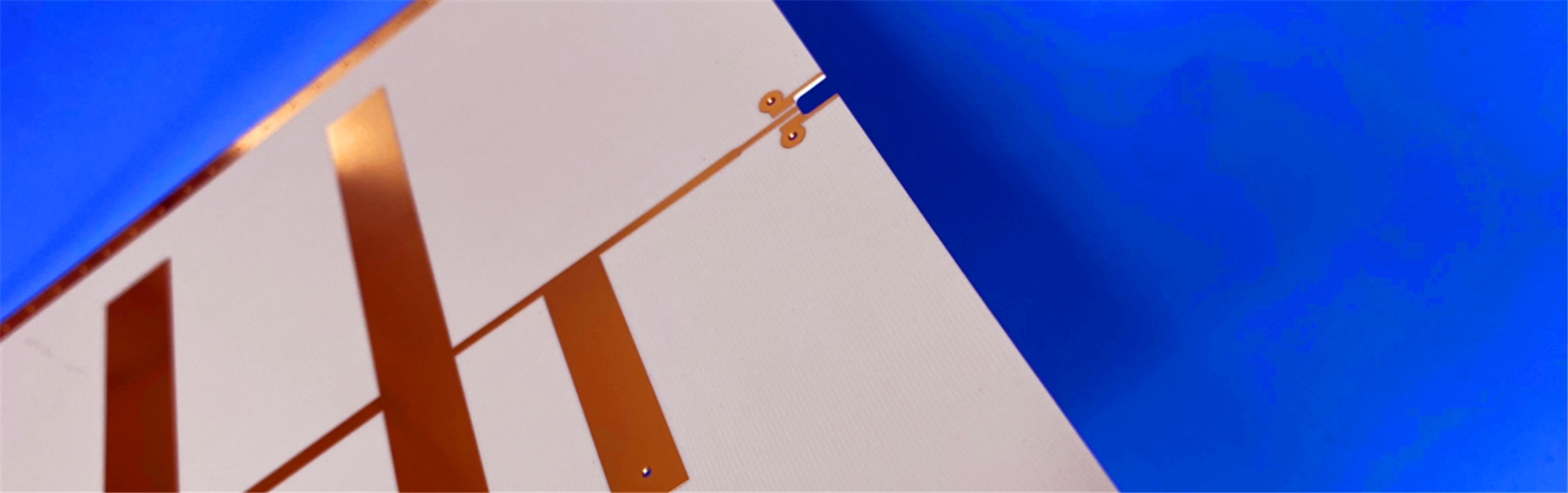
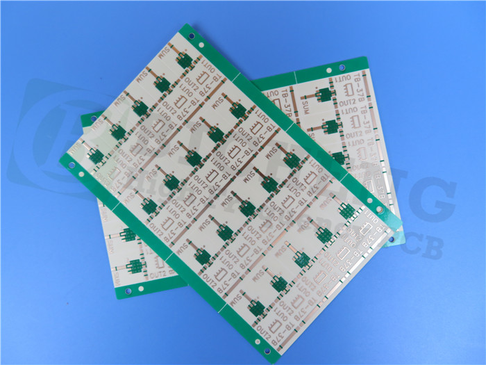
This 2-layer Rogers RO4725JXR PCB adopts a specific stackup configuration, consisting of a 35 μm copper_layer_1, a Rogers RO4725JXR Core with a thickness of 30.7 mils (equivalent to 0.780 mm), and a 35 μm copper_layer_2. The finished thickness of the board reaches 0.9 mm, while the finished copper weight on the outer layers is 1 oz (corresponding to 1.4 mils).
In terms of construction details, RO4725JXR PCB has dimensions of 146.15 mm × 60.8 mm. It features a minimum trace/space of 5/6 mils and a minimum hole size of 0.5 mm. Notably, this PCB does not incorporate blind vias, and the via plating thickness is set at 20 μm.
For surface treatment and markings, RO4725JXR PCB employs immersion gold as its surface finish. It is equipped with a green solder mask on the top layer, while no solder mask is applied to the bottom layer. Additionally, neither top nor bottom silkscreen is present on the board.
To guarantee quality, a 100% electrical test is conducted on the PCB before shipment. The provided artwork for manufacturing is in the format of Gerber RS-274-X files, and the PCB complies with the IPC-Class-2 quality standard. This product is available for global distribution.
In terms of component and connection details, the PCB accommodates a total of 54 components and 67 pads. Specifically, there are 67 SMT pads on the top layer, with no SMT pads on the bottom layer. It also includes 249 vias and 3 nets. This PCB is typically utilized in applications such as Cellular Base Station Antennas and Power Amplifiers.
Rogers RO4725JXR PCB specifications
| Parameters | Values |
| PCB Type | 2-layer rigid PCB |
| Copper_layer_1 | 35 μm |
| Rogers RO4725JXR Core | 30.7mil (0.780 mm) |
| Copper_layer_2 | 35 μm |
| Board Dimensions | 146.15mm x 60.8mm = 20PCS, +/- 0.15mm |
| Minimum Trace/Space | 5/6 mils |
| Minimum Hole Size | 0.5mm |
| Blind vias | No |
| Finished Board Thickness | 0.9mm |
| Finished Cu Weight | 1oz (1.4 mils) outer layers |
| Via Plating Thickness | 20 μm |
| Surface Finish | Immersion Gold |
| Top Silkscreen | No |
| Bottom Silkscreen | No |
| Top Solder Mask | Green |
| Bottom Solder Mask | No |
| Electrical Test | 100% prior to shipment |
| Components | 54 |
| Total Pads | 67 |
| Thru Hole Pads | 0 |
| Top SMT Pads | 67 |
| Bottom SMT Pads | 0 |
| Vias | 249 |
| Nets | 3 |
| Type of Artwork Supplied | Gerber RS-274-X |
| Quality Standard | IPC-Class-2 |
| Availability | Worldwide |
| Typical Applications | Cellular Base Station Antennas and Power Amplifiers |
Features/Benefits:
RO4725JXR RF PCBs offer a range of advantages due to their unique properties:
Reduced PIM: These PCBs exhibit reduced passive inter-modulation, resulting in improved signal quality and reduced interference.
Low insertion loss: With low loss dielectric and low profile foil, these PCBs minimize signal loss during transmission.
RO4725JXR Dk 2.55: The dielectric constant of 2.55 ensures consistent electrical performance and compatibility with standard PTFE-based materials.
The PCBs also feature unique filler and closed microspheres, providing additional benefits:
Low density: With a density of only 1.27 gm/cm3, these PCBs are approximately 30% lighter than PTFE/Glass boards, offering weight savings in applications.
Low Z-axis CTE (Coefficient of Thermal Expansion) of 25.6ppm/°C: This property ensures dimensional stability and reliable performance across temperature variations.
Other notable features include:
High Tg (>280°C): The high glass transition temperature allows for design flexibility and compatibility with automated assembly processes.
Low TCDk (+34 ppm/°C): The low thermal coefficient of dielectric constant ensures consistent circuit performance, minimizing variations due to temperature changes.
Specially formulated thermoset resin system/filler: This formulation offers ease of fabrication and compatibility with plated through-hole (PTH) processes.
In addition, RO4725JXR laminates are environmentally friendly:
Lead-free process compatibility: These PCBs are suitable for lead-free soldering processes.
RoHS compliant: They meet the requirements of the Restriction of Hazardous Substances (RoHS) directive.
Typical applications for RO4725JXR PCBs include Cellular Base Station Antennas etc.
PCB Capability 2023
| Factory Process Capability (2023) | |
| Substrate Types and Brands | Standard FR-4, High Tg FR-4, High Frequency Materials, Polyimide/PET flexible Materials |
| Shengyi, ITEQ, Isola, Taiwan Union, Rogers Corp. Taconic, Panasonic | |
| Board Types | Rigid PCB, Flexible Circuits, Rigid-Flex PCB, Hybrid PCB, HDI PCB |
| CCL Model | High Tg FR-4: S1000-2M, TU-872 SLK, TU-768, IT-180A High CTI FR-4: S1600L, ST115 |
| Rogers Corp: RO4350B, RO4003C, RO4730G3, RO4360G2, RO4533, RO4534, RO4535, RO4835, RO3003, RO3006, RO3010, RO3035, RO3203, RO3210; RT/Duriod 5880; RT/Duriod 5870, RT/Duriod 6002, RT/Duroid 6010, RT/duroid 6035HTC; RT/duroid 5880LZ; TMM3, TMM4, TMM6, TMM10, TMM10i, TMM13i, Kappa 438; AD250C, AD255C, AD300D, AD350A, AD450, AD600, AD1000, TC350; TC600; DiClad 880, DiClad 870, DiClad 527; IsoClad 917 | |
| Taconic: TLF-35; RF-35TC, RF-60A, RF-60TC, RF-35A2, RF-45, RF-10, TRF-45; TLX-0, TLX-6, TLX-7, TLX-8; TLX-9, TLY-3, TLY-5, TLY-5Z; | |
| F4B PTFE Composites: (DK2.2 DK2.65 DK2.85 DK2.94, DK3.0, DK3.2, DK3.38, DK3.5, DK4.0, DK4.4, DK6.15, DK10.2) | |
| Maximum Delivery Size | 1200mm x 572 mm |
| Minimum Finished Board Thickness | L≤2L: 0.15mm; 4L: 0.4mm |
| Maximum Finished Board Thickness | 10.0 mm |
| Blind Buried Holes (Non-crossing) | 0.1mm |
| Maximum Hole Aspect Ratio | 15:01 |
| Minimum Mechanical Drill Hole Diameter | 0.1 mm |
| Through-hole Tolerance | +/- 0.0762 mm |
| Press-fit Hole Tolerance | +/- 0.05mm |
| Non-plated Copper Hole Tolerance | +/- 0.05mm |
| Maximum Number of Layers | 32 |
| Internal and External Layer Maximum Copper Thickness | 12Oz |
| Minimum Drill Hole Tolerance | +/- 2mil |
| Minimum Layer-to-Layer Tolerance | +/- 3mil |
| Minimum Line Width/Spacing | 3mil/3mil |
| Minimum BGA Diameter | 8mil |
| Impedance Tolerance | < 50Ω ±5Ω; ≥50Ω±10% |
| Surface Treatment Processes | Leaded/Lead-free HASL, Immersion Gold, Immersion Silver, Immersion Tin, OSP, ENIG, ENEPIG, Carbon Ink, Peelable Mask, Gold Finger, etc. |