

 Home
-
Prototype PCB
-
12-Layer Impedance Controlled HDI PCB on High Tg FR-4 with ENIG Surface Finish
Home
-
Prototype PCB
-
12-Layer Impedance Controlled HDI PCB on High Tg FR-4 with ENIG Surface Finish
12-Layer Impedance Controlled HDI PCB on High Tg FR-4 with ENIG Surface Finish
Printed Circuit Boards are custom-made products; the images and specifications provided are for reference only.
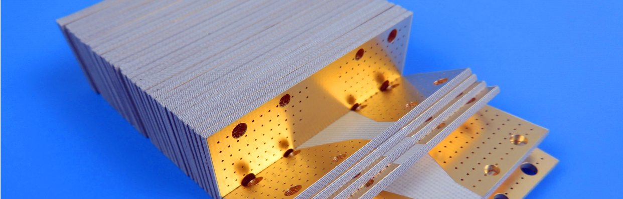
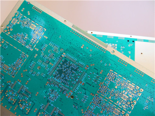
General Description
This is a 12-layer impedance controlled PCB designed for high-speed signal transmission applications. Fabricated on high Tg 175°C FR-4 material from ITEQ, the board has a finished thickness of 2.0mm and features a 2+N+2 HDI via structure.
The Multilayer PCB is supplied with a green solder mask and white silkscreen, both from Taiyo, while contact pads are coated with immersion gold (ENIG). Controlled impedance is maintained for both single-ended signals and differential pairs on critical layers. The HDI PCBs are manufactured per IPC-6012 Class 2 standards based on provided Gerber files. Each shipment unit consists of 20 boards, packaged individually, and the panel is supplied in a single-up configuration.
Signal Trace Impedance Control
Trace Layer |
Trace Width (mil) |
Trace Impedance (Ohm) |
Precision |
Reference Layer |
Top Layer |
4 |
50 |
±10% |
Mid-Layer 1 |
L03, Mid-Layer 2 |
4 |
50 |
±10% |
Mid-Layer 1 |
L10, Mid-Layer 9 |
4 |
50 |
±10% |
Mid-Layer 7, Mid-Layer 10 |
Bottom Layer |
4 |
50 |
±10% |
Mid-Layer 10 |
Differential Pairs Impedance Control
Layer |
Trace Width / Space (Mil) |
Trace Impedance (Ohm) |
Precision |
Frequency (MHz) |
Top Layer |
3.1 / 5.5 |
100 |
±10% |
Mid-Layer 1 |
Top Layer |
4.0 / 5.1 |
90 |
±10% |
Mid-Layer 1 |
L03, Mid-Layer 2 |
3.1 / 5.9 |
100 |
±10% |
Mid-Layer 1, Mid-Layer 4 |
L06, Mid-Layer 5 |
4.0 / 7.4 |
100 |
±10% |
Mid-Layer 4, Mid-Layer 6 |
L06, Mid-Layer 5 |
4.0 / 4.7 |
90 |
±10% |
Mid-Layer 4, Mid-Layer 6 |
L07, ,Mid-Layer 6 |
4.0 / 7.4 |
100 |
±10% |
Mid-Layer 5, Mid-Layer 7 |
L07, ,Mid-Layer 6 |
4.0 / 4.7 |
90 |
±10% |
Mid-Layer 5, Mid-Layer 7 |
L10, Mid-Layer 9 |
3.1 / 5.9 |
100 |
±10% |
Mid-Layer 7, Mid-Layer 10 |
Bottom Layer |
4.0 / 5.5 |
100 |
±10% |
Mid-Layer 10 |
Bottom Layer |
4.0 / 5.1 |
90 |
±10% |
Mid-Layer 10 |
Features and benefits
Lead free assemblies with a maximum reflow temperature of 260℃.
Long storage time ( It can be stored for more than 1 year in vacuum bag)
Improved the speed of signal transmission
PCB manufacturing on required specifications.
Quick and on-time delivery
UL recognized and RoHS Directive-compliant
Prototype PCB capability
Applications
Dsl Modem
Solar Battery Charger
Vehicle Tracker
GPS Receiver
Wi Fi Antenna
Bluetooth USB Hub
USB Wireless Router
SMS Modem
Multicoupler Antenna
Phone systems
Parameter and data sheet
| PCB SIZE | 257 x 171.5mm=1PCS=1design |
| BOARD TYPE | Multilayer PCB |
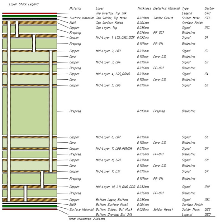
| Number of Layers | 12 Layers |
| Surface Mount Components | YES |
| Through Hole Components | YES |
| LAYER STACKUP | copper ------- TOP 17um(1oz)+plate 25um |
| 130 um prepreg 1080 x 2 | |
| copper ------- L02 32um(1oz) | |
| 150um core FR-4 | |
| copper ------- L03 18um(0.5oz) | |
| 130 um prepreg 1080 x 2 | |
| copper ------- L04 18um(0.5oz) | |
| 150um core FR-4 | |
| copper ------- L05 18um(0.5oz) | |
| 130 um prepreg 1080 x 2 | |
| copper ------- L06 18um(0.5oz) | |
| 813um core FR-4 | |
| copper ------- L07 18um(0.5oz) | |
| 130 um prepreg 1080 x 2 | |
| copper ------- L08 18um(0.5oz) | |
| 150um core FR-4 | |
| copper ------- L09 18um(0.5oz) | |
| 130 um prepreg 1080 x 2 | |
| copper ------- L10 18um(0.5oz) | |
| 150um core FR-4 | |
| copper ------- L11 35um(1oz) | |
| 130 um prepreg 1080 x 2 | |
| copper ------- BOT 17um(0.5oz)+plate 25um | |
| TECHNOLOGY | |
| Minimum Trace and Space: | 4 mil / 4 mil |
| Minimum / Maximum Holes: | 0.25 mm / 3.0 mm |
| Number of Different Holes: | 26 |
| Number of Drill Holes: | 4013 |
| Number of Milled Slots: | 0 |
| Number of Internal Cutouts: | 0 |
| Impedance Control | Single Signal Impedance and Differential Pairs Impedance |
| BOARD MATERIAL | |
| Glass Epoxy: | FR-4, ITEQ IT-180, Tg>175℃, er<5.4 |
| Final foil external: | 1oz |
| Final foil internal: | 1oz |
| Final height of PCB: | 2.0mm ±10% |
| PLATING AND COATING | |
| Surface Finish | Immersion Gold (ENIG)( 2 µ"" over 100 µ"" nickel) |
| Solder Mask Apply To: | Top and Bottom, 12micon Minimum. |
| Solder Mask Color: | Green, PSR-2000GT600D, Taiyo supplied. |
| Solder Mask Type: | LPSM |
| CONTOUR/CUTTING | Routing |
| MARKING | |
| Side of Component Legend | TOP |
| Colour of Component Legend | White, IJR-4000 MW300, Taiyo Supplied. |
| Manufacturer Name or Logo: | Marked on the board in a conductor and leged FREE AREA |
| VIA | Plated Through Hole(PTH), Blind via L1-L2, L11-L12, Buried via L2-L3, L3-L10, L10-L11, via tented. Vin in pad under BGA package |
| FLAMIBILITY RATING | UL 94-V0 Approval MIN. |
| DIMENSION TOLERANCE | |
| Outline dimension: | 0.0059"" (0.15mm) |
| Board plating: | 0.0030"" (0.076mm) |
| Drill tolerance: | 0.002"" (0.05mm) |
| TEST | 100% Electrical Test prior shipment |
| TYPE OF ARTWORK TO BE SUPPLIED | email file, Gerber RS-274-X, PCBDOC etc |
| SERVICE AREA | Worldwide, Globally. |
Impedance PCB and Impedance Match
Characteristic impedance is a critical parameter in printed circuit board design, particularly for high-frequency applications. The consistency and matching between the conductor's characteristic impedance and the requirements of active devices or signals must be carefully considered during the design phase, making impedance control a fundamental aspect of PCB reliability engineering.
As signal transmission rates increase with higher frequencies, various physical factors in the PCB manufacturing process—including etching variations, dielectric thickness, and copper track width—can cause impedance fluctuations that lead to signal distortion. Therefore, maintaining characteristic impedance within a specified tolerance range, commonly referred to as "impedance control," becomes essential in high-speed board design.
Key factors influencing PCB trace impedance include:
Copper trace width and thickness
Dielectric constant of the substrate material
Dielectric thickness between layers
Solder mask thickness and properties
Reference plane placement and return path consistency
Adjacent trace proximity and layout
Effective impedance management during design helps minimize signal reflection, electromagnetic interference, and signal integrity degradation, thereby ensuring stable performance in the final application. Designers can refer to established empirical formulas to calculate target impedance values for both microstrip and stripline configurations during the layout process.