

 Home
-
Multilayer PCB
-
IT-180 10-Layer HDI PCB High Temperature PCB with Immersion Gold and 100 ohm Impedance
Home
-
Multilayer PCB
-
IT-180 10-Layer HDI PCB High Temperature PCB with Immersion Gold and 100 ohm Impedance
IT-180 10-Layer HDI PCB High Temperature PCB with Immersion Gold and 100 ohm Impedance
Printed Circuit Boards are custom-made products; the images and specifications provided are for reference only.
General Description
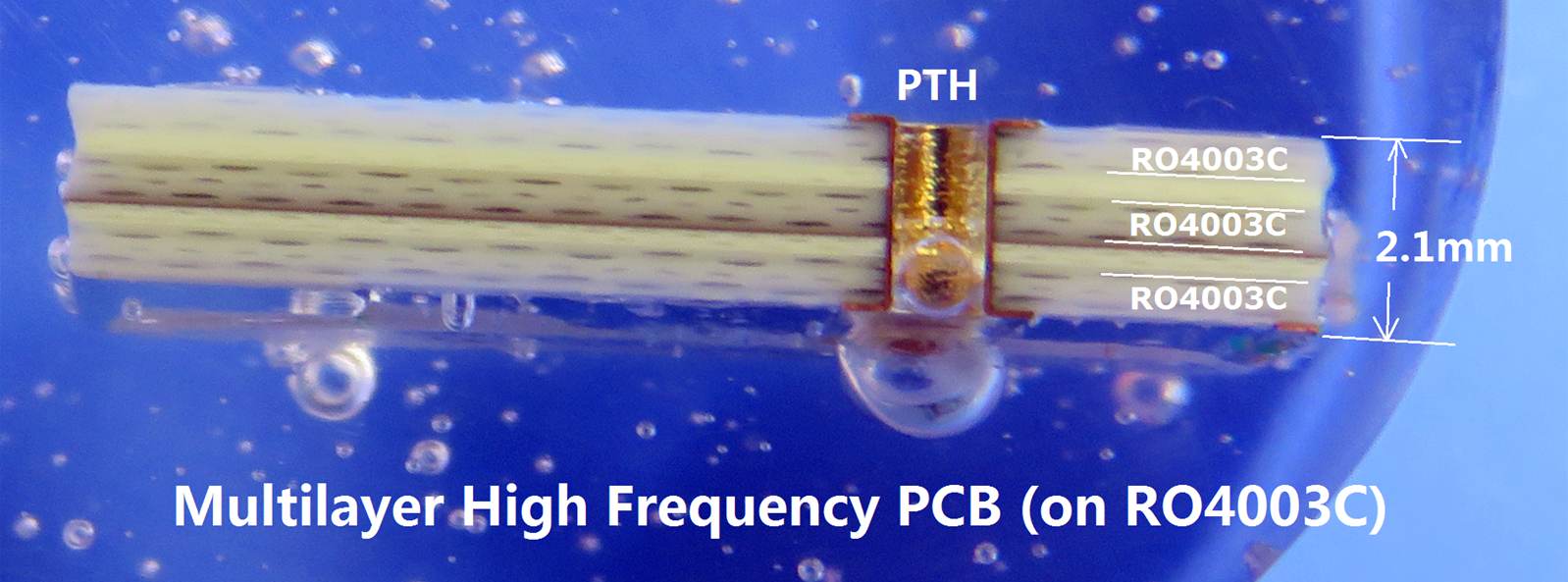
This is a 10-layer printed circuit board (PCB) constructed on ITEQ’s IT-180 FR-4 substrate (with a glass transition temperature, Tg, of 170℃), specifically designed for PLC control applications. IT-180 10-Layer HDI PCB has a finished thickness of 2.0 mm, featuring a green solder mask with white silkscreen and immersion gold plating on its pads. The PCB is supplied as a single-board unit.
Its high-density interconnection configuration includes blind vias (L1-L3, L7-L10) and buried vias (L3-L7). Impedance control of 100 ohms is implemented on the top layer, with a trace/space specification of 4 mils/5 mils.
All PCBs are fabricated in compliance with the IPC 6012 Class 2 standard, using the provided Gerber data for production. For shipment, each batch of 20 boards is vacuum-packed.
PCB Specifications
| Item | Description | Value | |||||||||||
| Layer count | 10 layer PCB | 10 layer board | |||||||||||
| Board type | Multilayer pcb | Multilayer pcb board | |||||||||||
| Board size | 168.38 x 273.34mm=1up | 168.38 x 273.34mm=1up | |||||||||||
| Laminate | Laminate Type | FR4 IT-180A | |||||||||||
| Supplier | ITEQ | ||||||||||||
| Tg | TG ≧170 | ||||||||||||
| Finished thickness | 2.0+/-10% MM | ||||||||||||
| Plating Thickness | PTH Cu thickness | >20 um | |||||||||||
| Inner layer Cu Thickness | 1/1 OZ | ||||||||||||
| Surface Cu thickness | 35 um | ||||||||||||
| Solder Mask | Material type | LP-4G G-05 | |||||||||||
| Supplier | Nan Ya | ||||||||||||
| Color | Green | ||||||||||||
| Single / both sides | Both Sides | ||||||||||||
| S/M thickness | >=10.0 um | ||||||||||||
| 3M tape test | NO Peel Off | ||||||||||||
| Legend | Material type | S-380W | |||||||||||
| Supplier | Tai yo | ||||||||||||
| Color | White | ||||||||||||
| Location | Both Sides | ||||||||||||
| 3M tape test | No peel off | ||||||||||||
| Circuit | Trace Width (mm) | 0.203+/-20%mm | |||||||||||
| Spacing (mm) | 0.203+/- 20%mm | ||||||||||||
| Identification | UL mark | 94V-0 | |||||||||||
| Date code | 1025 | ||||||||||||
| Mark location | CS | ||||||||||||
| Surface Treatment | ENIG | Nickel | 100u'' | ||||||||||
| Gold | ≧2u'' | ||||||||||||
| Reliabilty Tests | Thermal shock test | 288±5℃, 10sec ,3 cycles | |||||||||||
| solder abllity test | 245±5℃ | ||||||||||||
| Function | Electrioal Test | 233+/-5℃ | |||||||||||
| Standard | IPC_6012C CLASS 2 | 100% | |||||||||||
| Appearance | Visual inspection | 100% | |||||||||||
| warp and twist | <= 0.75% | ||||||||||||
| Vias | Through holes | L1-L10 | |||||||||||
| Blind vias & Buried vias | L1-L3, L7-L10, L3-L7 | ||||||||||||
| Drill table (mm) | No | PTH/NPTH | Size | ||||||||||
| 1 | Y | 0.500*1.00+/-0.075 | |||||||||||
| 2 | Y | 0.508+/-0.075 | |||||||||||
| 3 | Y | 0.610+/-0.075 | |||||||||||
| 4 | N | 0.700+/-0.075 | |||||||||||
| 5 | Y | 0.711+/-0.075 | |||||||||||
| 6 | Y | 0.914+/-0.075 | |||||||||||
| 7 | N | 1.118+/-0.075 | |||||||||||
| 8 | N | 1.219+/-0.075 | |||||||||||
| 9 | N | 1.524+/-0.075 | |||||||||||
| 10 | N | 1.600+/-0.075 | |||||||||||
| 11 | Y | 2.540+/-0.075 | |||||||||||
| 12 | Y | 2.997+/-0.075 | |||||||||||
| 13 | N | 3.500+/-0.075 |
Typical Applications
CCTV Security
Wireless G Router
Programmable Controllers
Automotive (Engine room ECU)
Multilayer and HDI PCB
Backplanes
Data Storage
Server and Networking
Telecommunications
Our Advantages
Engineering design prevents problems from occurring in pre-production;
ISO9001, ISO14001, ISO13485, IATF 16949, UL certified
Powerful PCB capabilities support your RD, sales and marketing;
Any Layer HDI PCBs;
16000㎡ workshop; 30000㎡ output/ month; 8000 types of PCB's/ month;
Customer complaint rate: <1%
Quick and on-time delivery;
No MOQ, low cost for prototypes and small runs quantity;
More than 22+ years of high frequency PCB experience.