

 Home
-
Multilayer PCB
-
4-Layer High Performance Multi-layer Polyimide PCB with Matte Black Mask and ENEPIG Surface Finish
Home
-
Multilayer PCB
-
4-Layer High Performance Multi-layer Polyimide PCB with Matte Black Mask and ENEPIG Surface Finish
4-Layer High Performance Multi-layer Polyimide PCB with Matte Black Mask and ENEPIG Surface Finish
Printed Circuit Boards are custom-made products; the images and specifications provided are for reference only.
General Description
1.1 General description
This multilayer PCB utilizes an FR-4 substrate with a Tg of 150°C and incorporates blind via technology, making it well-suited for mobile phone applications. The 1.6mm thick board features a green solder mask and white silkscreen (both from Taiyo) with immersion gold finish on pads. Constructed on ITEQ base material, it specifically employs blind vias from the top to inner layer 1 and from inner layer 3 to the bottom. All boards are fabricated to IPC-6012 Class 2 standards based on supplied Gerber data and are packaged in lots of 25 for shipment.
1.2 Features and Benefits
- Middle Tg FR-4 Shows low Z-CTE and excellent through hole reliability;
- Immersion gold has high solderability, no stressing and less contamination;
- Multilayer shortened connection between electronic components;
- 16000㎡ workshop and 8000 types of PCB's per month;
- Delivery on time: >98%
- No minimum order quantity. 1 piece is available;
1.3 Applications
Industrial Computer
GPS Tracking System
POS Cash Register
Embedded Systems
Data Acquisition System
Microcontrollers
PC and Notebook
1.4 Parameter and data sheet
| PCB SIZE | 119 x 80mm=1PCS | |
| BOARD TYPE | Multilayer PCB | |
| Number of Layers | 4 layers | |
| Surface Mount Components | YES | |
| Through Hole Components | YES | |
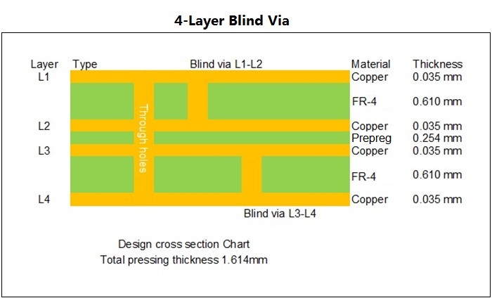
| LAYER STACKUP | copper ------- 18um(0.5oz)+plate TOP layer | |
| Core FR-4 0.61mm | ||
| copper ------- 35um(1oz) MidLayer 1 | ||
| Prepreg 0.254mm | ||
| copper ------- 35um(1oz) MidLayer 2 | ||
| Core FR-4 0.61mm | ||
| copper ------- 18um(0.5oz)+plate BOT layer | ||
| TECHNOLOGY | ||
| Minimum Trace and Space: | 4 mil / 4 mil | |
| Minimum / Maximum Holes: | 0.3 mm /3.5 mm | |
| Number of Different Holes: | 9 | |
| Number of Drill Holes: | 415 | |
| Number of Milled Slots: | 0 | |
| Number of Internal Cutouts: | 0 | |
| Impedance Control: | no | |
| Number of Gold finger: | 0 | |
| BOARD MATERIAL | ||
| Glass Epoxy: | FR-4 Tg150℃, er<5.4.IT-158, ITEQ | |
| Final foil external: | 1oz | |
| Final foil internal: | 1oz | |
| Final height of PCB: | 1.6mm ±0.16 | |
| PLATING AND COATING | ||
| Surface Finish | Immersion Gold | |
| Solder Mask Apply To: | TOP and Bottom, 12micron Minimum | |
| Solder Mask Color: | Green, PSR-2000 GT600D, Taiyo Supplied. | |
| Solder Mask Type: | LPSM | |
| CONTOUR/CUTTING | Routing, stamp holes. | |
| MARKING | ||
| Side of Component Legend | TOP and Bottom. | |
| Colour of Component Legend | White, S-380W, Taiyo Supplied. | |
| Manufacturer Name or Logo: | Marked on the board in a conductor and leged FREE AREA | |
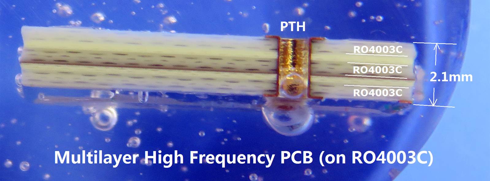
| VIA | Plated through hole(PTH), minimum size 0.3mm. Blind Via Top to Inner layer 1, Bottom to Inner layer 2 | |
| FLAMIBILITY RATING | UL 94-V0 Approval MIN. | |
| DIMENSION TOLERANCE | ||
| Outline dimension: | 0.0059"" | |
| Board plating: | 0.0029"" | |
| Drill tolerance: | 0.002"" | |
| TEST | 100% Electrical Test prior shipment | |
| TYPE OF ARTWORK TO BE SUPPLIED | email file, Gerber RS-274-X, PCBDOC etc | |
| SERVICE AREA | Worldwide, Globally. |
1.5 Composition of Holes
The blind hole is located on the top and bottom surface of the printed circuit board and has a certain depth for the connection between the surface line and the inner line below. The depth of the hole usually does not exceed a certain ratio (aperture). Buried hole is a connecting hole located in the inner layer of the printed circuit board, which does not extend to the surface of the circuit board.
The above two kinds of holes are located in the inner layer of the circuit board. The formation of through hole process is used before lamination, and several inner layers may be overlapped done during the formation of the through hole.
The third is called a through hole, which passes through the entire circuit board. It can be used to interconnect internally or as an installation location hole for components. Because the through hole is easier to realize and the cost is low, it is used in most printed circuit boards instead of the other two. The following mentioned holes, without special instructions, are considered as through holes.
From the design point of view, a hole is mainly composed of two parts, one is the middle hole (drill hole), the other is the pad area around the hole, see below. The size of these two parts determines the size of the hole. Clearly, in
high-speed, high-density PCB design, designers always want the holes the smaller the better, so that it can leave more wiring space on the board.
| Factory Process Capability (2025) | |
| Substrate Types | Standard FR-4, High Tg FR-4, High Frequency Materials, Rigid Polyimide, Flexible Polyimide, Transparent PET Materials, AL2O3 Ceramic, AlN Ceramic etc. |
| Substrate Brands | Shengyi, ITEQ, KB, Isola, Taiwan Union, Rogers Corp. Taconic, Wangling, Panasonic etc |
| Board Types | Rigid PCB, Flexible Circuits, Rigid-Flex PCB, Hybrid PCB, HDI PCB, Heavy Copper, High Speed, High frequency etc. |
| Copper Clad Laminates(CCL) | High Tg FR-4: S1000-2M, TU-872 SLK, TU-768, TU-883, IT-180A, FR408HR, 370HR, High CTI FR-4: S1600L, ST115 High speed: M6 (R5775G Core / R-5670 Prepreg) |
| Rogers Corp: RO4350B, RO4003C, RO4725JXR, RO4730G3, RO4360G2, RO4533, RO4534, RO4535, RO4830, RO4835, RO3003, RO3006, RO3010, RO3035, RO3203, RO3210; RT/Duriod 5880; RT/Duriod 5870, RT/Duriod 6002, RT/duroid 6006, RT/Duroid 6010.2LM, RT/duroid 6035HTC; RT/duroid 5880LZ, RT/duroid 6202; TMM3, TMM4, TMM6, TMM10, TMM10i, TMM13i, Kappa 438; AD250C, AD255C, AD300D, AD350A, AD450, AD600, AD1000, TC350; TC600; DiClad 880, DiClad 870, DiClad 527; IsoClad 917, IsoClad 933; CLTE-XT, CLTE-AT, CLTE-MW; CuClad 217, CuClad 233, CuClad 250. | |
| Taconic: TLF-35; RF-35TC, RF-60A, RF-60TC, RF-35A2,RF-30, RF-35, RF-45, RF-10, TRF-45; TLX-0, TLX-6, TLX-7, TLX-8; TLX-9, TLY-3, TLY-5, TLY-5Z; CER-10; TSM-DS3 | |
| Wangling: F4BM217, F4BM220, F4BM233, F4BM245, F4BM255, F4BM265, F4BM275, F4BM294, F4BM300; F4BME217, F4BME220, F4BME233, F4BME245, F4BME255, F4BME265, F4BME275, F4BME294, F4BME300; F4BTM298, F4BTM300, F4BTM320, F4BTM350; F4BTME298, F4BTME300, F4BTME320, F4BTME350; TP300, TP440, TP600, TP615, TP960, TP1020, TP1100, TP1600, TP2000, TP2200, TP2500; TF300, TF440, TF600, TF960, TF1020, TF1600; F4BTMS220, F4BTMS233, F4BTMS255, F4BTMS265, F4BTMS294, F4BTMS300, F4BTMS350, F4BTMS430, F4BTMS450, F4BTMS615, F4BTMS1000; TFA294, TFA300, TFA615, TFA1020; WL-CT300, WL-CT330, WL-CT330Z, WL-CT338, WL-CT350, WL-CT440, WL-CT615. |
|
| Maximum Delivery Size | 1200mm x 572 mm |
| Minimum Finished Board Thickness | L≤2L: 0.15mm; 4L: 0.4mm |
| Maximum Finished Board Thickness | 10.0 mm |
| Blind Buried Holes (Non-crossing) | 0.1mm |
| Maximum Hole Aspect Ratio | 15:01 |
| Minimum Mechanical Drill Hole Diameter | 0.1 mm |
| Through-hole Tolerance | +/- 0.0762 mm |
| Press-fit Hole Tolerance | +/- 0.05mm |
| Non-plated Copper Hole Tolerance | +/- 0.05mm |
| Maximum Number of Layers | 32 |
| Internal and External Layer Maximum Copper Thickness | 12Oz |
| Minimum Drill Hole Tolerance | +/- 2mil |
| Minimum Layer-to-Layer Tolerance | +/- 3mil |
| Minimum Line Width/Spacing | 3mil/3mil |
| Minimum BGA Diameter | 8mil |
| Impedance Tolerance | < 50Ω ±5Ω; ≥50Ω±10% |
| Special Technology | High density interconnection (HDI), Hybrid design/ mixed PCB, Blind/Buried vias, Resin filled / copper filled and capped, Copper coin embedded, Staircase PCB, Edge plated PCB, Heavy copper PCB, Half holes/castled Edge holes, Thick PCB etc |
| Surface Treatment Processes | Leaded/Lead-free HASL, Immersion Gold, Immersion Silver, Immersion Tin, OSP, ENIG, ENEPIG, Pure gold, Carbon Ink, Peelable Mask, Gold Finger, etc. |