
 Home
Home
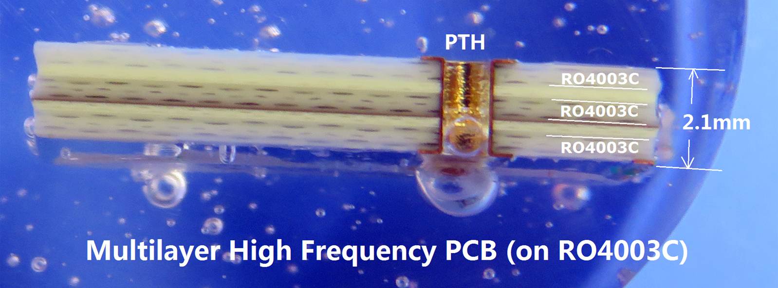
20-Layer 3.0mm Thick TU-883 HDI Immersion gold PCB With 50 Ohm Impedance
Printed Circuit Boards are custom-made products; the images and specifications provided are for reference only.
General Description
This is a low-loss, high-performance multi-layer printed circuit board (PCB) constructed using TUC’s TU-883 core, featuring 20 copper layers (i.e., a 20-layer PCB). Copper foils of 1 oz and 0.5 oz are used alternately across the layers.
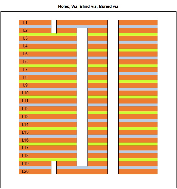
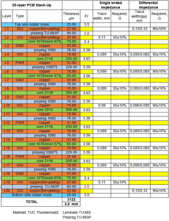
TU-883 PCB has an overall thickness of 3.0 mm, with immersion gold plating on its pads, a green solder mask, and white silkscreen. Its design includes a High-Density Interconnect (HDI) configuration, incorporating blind vias (from the top layer to inner layer 1, and from inner layer 18 to the bottom layer) as well as buried vias (from inner layer 1 to inner layer 18).
Additionally, this is an impedance-controlled PCB: 50 Ohms of impedance is maintained on each signal layer, with a tolerance of ±10%. All PCBs are fabricated in compliance with the IPC-Class 2 standard, and they are vacuum-packed for shipment, with 10 boards per pack.
.jpg)
PCB Specifications
| Item | Properties | Value | ||||||||||||
| 1. Laminate | Material Type | TU-883 | ||||||||||||
| Tg | 170℃ | |||||||||||||
| Supplier | TUC | |||||||||||||
| Thickness | 2.8-3.1mm | |||||||||||||
| 2.Plating thickness | Hole Wall | 26.51µm | ||||||||||||
| Outer copper | 41.09µm | |||||||||||||
| Inner Copper | 15µm / 31µm | |||||||||||||
| 3.Solder mask | Material Type | TAIYO/ PSR-2000GT600D | ||||||||||||
| Color | Green | |||||||||||||
| Rigidity (Pencil Test) | 5H | |||||||||||||
| S/M Thickness | 20.11µm | |||||||||||||
| Location | Both Sides | |||||||||||||
| 4. Component Mark | Material Type | IJR-4000 MW300 | ||||||||||||
| Color | White | |||||||||||||
| Location | C/S, S/S | |||||||||||||
| 5. Vias | Throught holes | L1-L20 | ||||||||||||
| Blind vias | L1-L2, L18-L20 | |||||||||||||
| Buried vias | L2-L19 | |||||||||||||
| 6. Identification | UL Mark | YES | ||||||||||||
| Date Code | 1025 | |||||||||||||
| Mark Location | Solder Side | |||||||||||||
| 7. Surface Finish | Method | Immersion Gold | ||||||||||||
| Nickel Thickness | 4.06µm | |||||||||||||
| Gold Thickness | 0.056µm | |||||||||||||
| 8. Normativeness | RoHS | Directive 2015/863/EU | ||||||||||||
| REACH | Directive 1907 /2006 | |||||||||||||
| 9.Annular Ring | Min. Line Width (mil) | 4.8mil | ||||||||||||
| Min. Spacing (mil) | 5.2mil | |||||||||||||
| 10.V-groove | Angle | / | ||||||||||||
| Residual thickness | / | |||||||||||||
| 11. Beveling | Angle | / | ||||||||||||
| Height | / | |||||||||||||
| 12. Function | Electrical Test | 100% PASS | ||||||||||||
| 13. Appearance | IPC Class Level | IPC-A-600J &6012D Class 2 | ||||||||||||
| Visual Inspection | IPC-A-600J &6012D Class 2 | |||||||||||||
| Warp and Twist | 0.21% | |||||||||||||
| 14. Reliability Test | Tape Test | No Peeling | ||||||||||||
| Solvent Test | No Peeling | |||||||||||||
| Solderability Test | 265 ±5℃ | |||||||||||||
| Thermal Stress Test | 288 ±5℃ | |||||||||||||
| Ionic Contamination Test | 0.56µg/c㎡ |
Stackup & Impedance Controlled
HDI vias