
 Home
-
Multilayer PCB
-
14-Layer High Density Interconnect (HDI) PCB Built on FR-4 Tg170℃ Substrate With ENIG Surface Finish
Home
-
Multilayer PCB
-
14-Layer High Density Interconnect (HDI) PCB Built on FR-4 Tg170℃ Substrate With ENIG Surface Finish
14-Layer High Density Interconnect (HDI) PCB Built on FR-4 Tg170℃ Substrate With ENIG Surface Finish
Printed Circuit Boards are custom-made products; the images and specifications provided are for reference only.
General Description
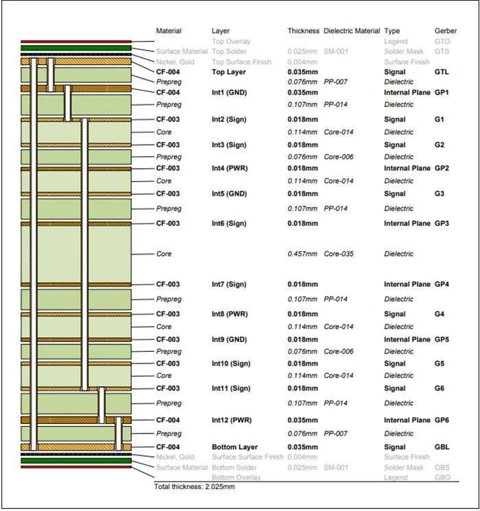
This 14-layer HDI printed circuit board (PCB) is constructed using an FR-4 Tg170℃ substrate, specifically designed for codec equipment applications. It has a finished thickness of 2.0 mm, with a green solder mask paired with white silkscreen, and immersion gold plating applied to its pads.
Key structural features include high-density interconnection layers, supported by blind vias (L1-L2, L13-L14), buried vias (L3-L4, L4-L12, L12-L13), and stacked microvias across different layers. The FR-4 Tg170℃ base material is sourced from ITEQ, and the PCB is manufactured as 1 unit per panel.
All boards are fabricated in compliance with the IPC 6012 Class 2 standard, using the provided Gerber data for production. For shipping, the PCBs are packaged in batches of 20 panels per pack.
.jpg)
Our Advantages
1. ISO9001, ISO14001, IATF16949, UL Certified;
2. Prototype to volume Production Capability;
3. 16000㎡ workshop;
4. 30000㎡ output capability per month;
5. 8000 types of PCB's per month;
6. IPC Class 2 / IPC Class 3;
7. Eligible products rate of first production: >95%
Applications of HDI PCBs
Automotive, GPS Trackers
5G WiFi, Embedded Systems Basics
Smartphones and tablets
Wearable technology and Healthcare
Access Control Solutions and Aerospace
Parameter and data sheet
| Number of Layers | 14-Layer | ||
| Board Type | Multilayer PCB | ||
| Board size | 220mm x 170mm=4PCS | ||
| Board Thickness | 2.0 mm +/-0.16 | ||
| Board Material | FR-4 | ||
| Board Material Supplier | ITEQ | ||
| Tg Value of Board Material | 170℃ | ||
| PTH Cu thickness | ≥20 um | ||
| Inner Iayer Cu thicknes | 18 um (0.5oz) | ||
| Surface Cu thickness | 35 um (1oz) | ||
| Solder Mask Type and Model No. | LPSM, PSR-2000GT600D | ||
| Solder Mask Supplier | TAIYO | ||
| Solder Mask Colour | Green | ||
| Number of Solder Masks | 2 | ||
| Thickness of Solder Mask | 14 um | ||
| Type of Silkscreen Ink | IJR-4000 MW300 | ||
| Supplier of Silkscreen | TAIYO | ||
| Color of Silkscreen | White | ||
| Number of Silkscreen | 1 | ||
| Mininum Trace (mil) | 5.8 mil | ||
| Minimum Gap(mil) | 6.2 mil | ||
| Surface Finish | Immersion Gold | ||
| RoHS Required | Yes | ||
| Warpage | 0.25% | ||
| Vias | Blind vias L1-L2, L13-L14, buried vias L3-L4, L4-L12, and L12-L13, Through holes. | ||
| Thermal Shock Test | Pass, 288±5℃,10 seconds, 3 cycles. No delamination, no blistering. | ||
| Solderablity Test | Pass, 255±5℃,5 seconds Wetting Area Least 95% | ||
| Function | 100% Pass electrical test | ||
| Workmanship | Compliance with IPC-A-600H & IPC-6012C Class 2 |
Different Types of HDI PCBs
To simplify the high density interconnect PCB, we define 3 types of HDI PCBs as below:
1+N+1, PCBs contain 1-time laser drill and pressing in the HDI boards.
I+N+I (I≥2), PCBs contain 2-time laser drill and pressing or more times laser drill and pressing, including the microvias staggered or stacked on different layers.
Any layer HDI, blind vias and buried vias can be freely put on different layers as designer want.