

 Home
-
High Temperature PCB
-
High Temperature PCB - Hard Gold Contact Fingers PCB - HDI Gold Finger PCB - Gold-plated Edge Connector Circuit Board
Home
-
High Temperature PCB
-
High Temperature PCB - Hard Gold Contact Fingers PCB - HDI Gold Finger PCB - Gold-plated Edge Connector Circuit Board
High Temperature PCB - Hard Gold Contact Fingers PCB - HDI Gold Finger PCB - Gold-plated Edge Connector Circuit Board
Printed Circuit Boards are custom-made products; the images and specifications provided are for reference only.
General Description
This 8-layer printed circuit board (PCB) is constructed on an FR-4 substrate with a glass transition temperature (Tg) of 170°C, specifically designed for Mobile Broadband use. It has a finished thickness of 1.6 mm, with a green Taiyo solder mask, white Taiyo silkscreen, and immersion gold plating on pads. The board features 80 gold finger strips along its edge for plug-in connectivity.
The base material is sourced from Taiwan ITEQ, with one PCB (1-up configuration) per manufacturing panel. It incorporates blind vias (connecting the top layer to inner layer 6) and buried vias (connecting inner layer 3 to inner layer 6), and is fabricated in compliance with the IPC 6012 Class 2 standard using customer-supplied Gerber data. For shipment, PCBs are packaged in batches of 25 units each.
.jpg)
Features and benefits
1. High Tg material shows excellent thermal reliability and CAF resistance providing long-term reliability for industrial and automobile application;
2. Gold fingers reduce contact resistance;
3. 16000㎡ workshop;
4. Meeting your PCB needs from prototype to mass production.
5. Strict WIP inspection and monitoring as well as working instruction;
6. IPC Class 2 / IPC Class 3;
7. ISO9001, ISO14001, ISO13485, UL certified manufacturing factory;
8. Diversified shipping method: FedEx, DHL, TNT, EMS;
9. No MOQ, low cost for prototypes and small runs quantity.
PCB Specifications
| PCB SIZE | 150 x 141mm=1PCS |
| BOARD TYPE | Multilayer PCB |
| Number of Layers | 8 layers |
| Surface Mount Components | YES |
| Through Hole Components | NO |
| LAYER STACKUP | copper ------- 18um(0.5oz)+plate TOP layer |
| Prepreg 7628(43%) 0.195mm | |
| copper ------- 35um(1oz) MidLayer 1 | |
| FR-4 0.2mm | |
| copper ------- 35um(1oz) MidLayer 2 | |
| Prepreg 7628(43%) 0.195mm | |
| copper ------- 35um(1oz) MidLayer 3 | |
| FR-4 0.2mm | |
| copper ------- 35um(1oz) MidLayer 4 | |
| Prepreg 7628(43%) 0.195mm | |
| copper ------- 35um(1oz) MidLayer 5 | |
| FR-4 0.2mm | |
| copper ------- 35um(1oz) MidLayer 6 | |
| Prepreg 7628(43%) 0.195mm | |
| copper ------- 18um(0.5oz)+plate BOT Layer | |
| TECHNOLOGY | |
| Minimum Trace and Space: | 4mil/4mil |
| Minimum / Maximum Holes: | 0.35/3.5mm |
| Number of Different Holes: | 23 |
| Number of Drill Holes: | 183 |
| Number of Milled Slots: | 0 |
| Number of Internal Cutouts: | 0 |
| Impedance Control | no |
| Number of Gold finger | 39 |
| BOARD MATERIAL | |
| Glass Epoxy: | FR-4, ITEQ IT-180 TG170℃ er<5.4 |
| Final foil external: | 1oz |
| Final foil internal: | 1oz |
| Final height of PCB: | 1.6mm ±0.16 |
| PLATING AND COATING | |
| Surface Finish | Immersion gold on pad, electroplated gold on edge connectors |
| Solder Mask Apply To: | TOP and Bottom, 12micron Minimum |
| Solder Mask Color: | Gloss Green, Taiyo PSR-2000GT600D |
| Solder Mask Type: | LPSM |
| CONTOUR/CUTTING | Routing |
| MARKING | |
| Side of Component Legend | TOP and Bottom. |
| Colour of Component Legend | White, Taiyo IJR-4000 MW300 |
| Manufacturer Name or Logo: | Marked on the board in a conductor and leged FREE AREA |
| VIA | Plated through hole(PTH), Blind via, Buried vias |
| FLAMIBILITY RATING | UL 94-V0 Approval MIN. |
| DIMENSION TOLERANCE | |
| Outline dimension: | 0.0059"" |
| Board plating: | 0.0029"" |
| Drill tolerance: | 0.002"" |
| TEST | 100% Electrical Test prior shipment |
| TYPE OF ARTWORK TO BE SUPPLIED | email file, Gerber RS-274-X, PCBDOC etc |
| SERVICE AREA | Worldwide, Globally. |
Applications
Bluetooth Transmitter
HDMI Splitters
CCTV Systems
Led Street Lights
Low Noise Amplifier
Door Access Control System
5G Mobile Hotspot
Multicoupler
Embedded Systems Development
Smart Phone and Cell Phone
Gold finger PCB
Purpose & Plating Process
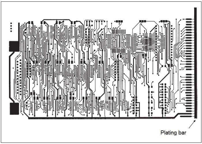
Gold finger PCBs eliminate the need for a two-part connector system by enabling direct electrical connection to the board. The nickel and gold plating process follows the same electrolytic deposition principle as copper or tin/lead plating, and can be performed manually or automatically.
Manual Plating: Boards remain relatively stationary in the gold plating bath, leading to uneven gold deposition along the contact finger row. Typically, the outermost fingers may have twice the gold thickness of the center fingers.
Automatic Plating: Boards slide through the plating cell during processing, ensuring consistent treatment of all contact fingers. This method controls gold thickness variation to within ±5% or better.
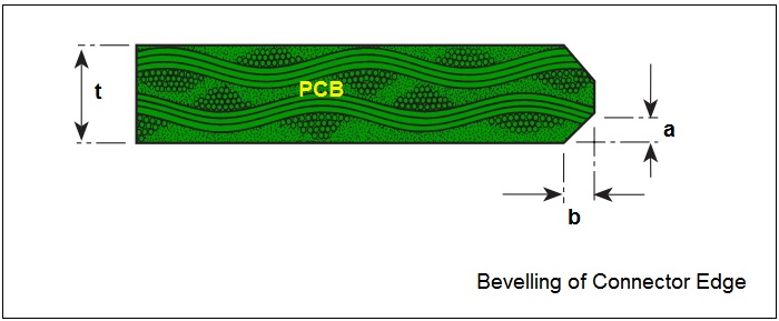
Edge Connector Design Features
Guiding & Polarization Slots: Edge connectors often include a slot to guide the PCB into the receptacle (locating slot) and prevent incorrect insertion (polarization slot). PCB manufacturers typically route this slot simultaneously with board contouring, requiring the slot to be slightly wider than the router bit used.
Bevelled Edge: The edge of the connector is bevelled to simplify insertion into the receptacle. This design also reduces scraping of the receptacle’s contacts during PCB insertion, minimizing wear on both components.