
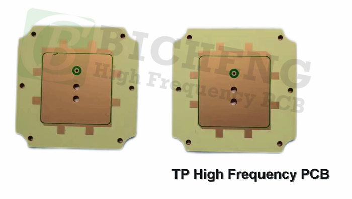
TP High Frequency PCB Material Introduction TP PCB material is a unique high-frequency thermoplastic material in the industry. The dielectric layer of TP-type laminates consists of ceramics and polyphenylene Oxide resin (PPO), without fiberglass reinforcement. The dielectric constant can be precisely adjusted by adjusting the ratio between ceramics and PPO resin. The production process is special, and it has excellent dielectric performance and high reliability. TP refers to the smooth surface material without copper cladding, TP-1 refers to the material with copper cladding on one side, and TP-2 refers to the material with copper cladding on both sides. Product Features: 1.The dielectric constant can be arbitrarily selected within the range of 3 to 25 according to circuit requirements, and it is stable. Common dielectric constants include 3.0, 4.4, 6.0, 6.15, 9.2, 9.6, 10.2, 11, 16, and 20. The dielectric loss is low, and the loss increases as the frequency increases, but the change is not significant within 10 GHz. 2.Long-term operating temperature ranges from -100°C to +150°C. It has excellent low-temperature resistance. When the temperature exceeds 180°C, the material may deform, the copper foil may peel off, and there may be significant changes in electrical performance. 3.The thinnest thickness is 0.5mm, and it is available in various thicknesses and can be customized. 4.It is resistant to radiation and has low outgassing. 5.Ideal material for Beidou, missile-borne, fuze, and miniaturized antennas. 6.The adhesion between copper foil and dielectric is more reliable than ceramic substrates with vacuum coating. The material is easy to machine and can be processed through drilling, turning, grinding, shearing, etching, and other methods, which ceramic substrates cannot achieve. 7.Convenient for PCB processing, it can be processed using methods suitable for thermoplastic materials, resulting in high yield and reduced processing cost compared to ceramic substrates. Due to the characteristics of the material, it is generally not recommended for multilayer PCB processing. If multilayer PCB processing is required, low-temperature bonding sheets should be selected, and feasibility should be fully considered Data Sheet Let's go through each parameter and its corresponding values: Dielectric Constant: TP300: The dielectric constant for TP300 is 3.0 with a tolerance of ±0.06. TP440: The dielectric constant for TP440 is 4.4 with a tolerance of ±0.09. TP600: The dielectric constant for TP600 is 6.0 with a tolerance of ±0.12. TP615: The dielectric constant is 6.15 with a tolerance of ±0.12. TP920: The dielectric constant is 9.2 with a tolerance of ±0.18. TP960: The dielectric constant is 9.6 with a tolerance of ±0.19. TP1020: The dielectric constant is 10.2 with a tolerance of ±0.2. TP1100: The dielectric constant is 11.0 with a tolerance of ±0.022. TP1600: The dielectric constant is 16.0 with a tolerance of ±0.4. TP2000: The dielectric constant is 20.0 with a tolerance of ±0.8. TP2200: The dielectric constant is 22.0 with a tolerance of ±0.88. TP2500: The dielectric constant is 25.0 with a tolerance of ±1.0. The dielectric constant can be customized within the range of 3.0 to 25 Dielectric Constant Tolerance: For dielectric constants ranging from 3.0 to 11.0, the tolerance is ±2%. For dielectric constants ranging from 11.1 to 16.0, the tolerance is ±2.5%. For dielectric constants ranging from 16.1 to 25.0, the tolerance is ±4%. Loss Tangent: Loss Tangent for dielectric constants ranging from 3.0 to 9.5 at 10GHz is 0.0010. Loss Tangent for dielectric constants ranging from 9.6 to 11.0 at 10GHz is 0.0012. Loss Tangent for dielectric constants ranging from 11.1 to 16.0 at 5GHz is 0.0015. Loss Tangent for dielectric constants ranging from 16.1 to 25.0 at 5GHz is 0.0020 to 0.0025. Dielectric Constant Temperature Coefficient: For dielectric constants ranging from 3.0 to 9.5, the temperature coefficient is -50 PPM/℃ (-55 ºC to 150 ºC). For dielectric constants ranging from 9.6 to 16.0, the temperature coefficient is -40 PPM/℃ (-55 ºC to 150 ºC). For dielectric constants ranging from 16.1 to 25.0, the temperature coefficient is -55 PPM/℃ (-55 ºC to 150 ºC). Peel Strength: Peel Strength in the normal state with 1 oz copper is greater than 0.6 N/mm. Peel Strength after AC humidity test with 1 oz copper is greater than 0.4 N/mm. Volume Resistivity: Volume Resistivity in the normal state at 500V is greater than 1×10^9 MΩ.cm. Surface Resistivity: Surface Resistivity in the normal state at 500V is greater than 1×10^7 MΩ. Coefficient of Thermal Expansion (XY Z): The coefficient of thermal expansion varies based on the dielectric constant range. Water Absorption: Water Absorption at 20±2℃ for 24 hours is less than or equal to 0.01%. Long-Term Operating Temperature: The long-term operating temperature range is from -100ºC to 150ºC. Material Composition: The laminate is composed of polyphenylene ether, ceramic, and paired with ED copper foil Product Technical Parameter Product Models & Data Sheet Product Features Test Conditions Unit TP TP-1 TP-2 Dielectric Constant When the dielectric constant is ≤11, the test condition is 10GHz. / 3.0±0.06 4.4±0.09 6.0±0.12 6.15±0.12 9.2±0.18 9.6±0.19 10.2±0.2 11.0±0.022 16.0±0.4 20.0±0.8 22.0±0.88 25.0±1.0 The dielectric constant can be customized within the range of 3.0 to 25. Dielectric Constant Tolerance Dielectric Constant 3.0~11.0 / ±2% Dielectric Constant 11.1~16.0 / ±2.5% Dielectric Constant 16.1~25.0 / ±4% Loss Tangent Loss Tangent?3.0~9.5 10GHz / 0.0010 Loss Tangent?9.6~11.0 10GHz / 0.0012 Loss Tangent 11.1~16.0 5GHz / 0.0015 Loss Tangent 16.1~25.0 5GHz / 0.0020~0.0025 Dielectric Constant Temperature Coefficient Dielectric Constant 3.0~9.5 -55 º~150ºC PPM/℃ -50 Dielectric Constant 9.6~16.0 -55 º~150ºC PPM/℃ -40 Dielectric Constant 16.1~25.0 -55 º~150ºC PPM/℃ -55 Peel Strength 1 OZ Normal State N/mm >0.6 1 OZ After AC Humidity Test N/mm >0.4 Volume Resistivity Normal State at 500V MΩ.cm >1×10^9 Surface Resistivity Normal State at 500V MΩ >1×10^7 Coefficient of Thermal Expansion Dielectric Constant 3.00~4.40 -55 º~150ºC PPM/℃ 60,60,70 Dielectric Constant 4.60~6.15 -55 º~150ºC PPM/℃ 50,50,60 Dielectric Constant 6.16~11.0 -55 º~150ºC PPM/℃ 40,40,55 Dielectric Constant 11.1~16.0 -55 º~150ºC PPM/℃ 40,40,50 Dielectric Constant 16.1~25.0 -55 º~150ºC PPM/℃ 35,35,40 Water Absorption 20±2℃, 24 hours % ≤0.01 Long-Term Operating Temperature High-Low Temperature Chamber ℃ -100º~150ºC Material Composition Polyphenylene ether, ceramic, paired with ED copper foil. The density and thermal conductivity data for materials with different dielectric constants are as follows: Product Features Unit Dielectric Constanct 3.0 4.4 6.0 6.15 9.6 10.2 11.0 16.0 20.0 22.0 25.0 Density g/cm3 1.69 1.89 2.1 2.12 2.26 2.33 2.40 2.76 2.73 2.77 2.94 Thermal Conductivity W/(M.K) 0.40 0.44 0.55 0.55 0.65 0.67 0.70 0.80 0.85 0.90 1.0 Our PCB Capability (TP Series) Our PCB manufacturing capabilities include: Layer count: We can manufacture single-sided and double-sided PCBs. Copper weight: We offer options for copper weight, including 1oz (35μm) and 2oz (70μm). Dielectric thickness (Dielectric thickness or overall thickness): We provide a range of dielectric thickness options, including 0.5mm, 0.8mm, 1.0mm, 1.2mm, 1.5mm, 2.0mm, 3.0mm, 4.0mm, 5.0mm, 6.0mm, 7.0mm, 8.0mm, 10.0mm, and 12.0mm. PCB size: Our manufacturing capabilities support PCB sizes up to 150mm X 220mm. Solder mask: We offer various solder mask colors, including Green, Black, Blue, Yellow, Red, and more. Surface finish: We provide a range of surface finish options, including Bare copper, HASL (Hot Air Solder Leveling), ENIG (Electroless Nickel Immersion Gold), Immersion silver, Immersion tin, OSP (Organic Solderability Preservative), Pure gold, ENEPIG (Electroless Nickel Electroless Palladium Immersion Gold), and more. Dielectric thickness (Dielectric thickness or overall thickness): The PCB can have dielectric thickness options of 0.635mm, 0.8mm, 1.0mm, 1.2mm, 1.5mm, 2.0mm, or 2.5mm. PCB Capability (TP Series) PCB Material: Polyphenylene ether, ceramic Designation (TP Series) Designation DK DF TP300 3.0±0.06 0.0010 TP440 4.4±0.09 0.0010 TP600 6.0±0.12 0.0010 TP615 6.15±0.12 0.0010 TP920 9.2±0.18 0.0010 TP960 9.6±0.2 0.0011 TP1020 10.2±0.2 0.0011 TP1100 11.0±0.22 0.0011 TP1600 16.0±0.32 0.0015 TP2000 20.0±0.4 0.0020 TP2200 22.0±0.44 0.0022 TP2500 25.0±0.5 0.0025 Layer count: Single Sided, Double Sided PCB Copper weight: 1oz (35µm), 2oz (70µm) Dielectric thickness (Dielectric thickness or overall thickness) 0.5mm, 0.8mm, 1.0mm, 1.2mm, 1.5mm, 2.0mm, 3.0mm, 4.0mm, 5.0mm, 6.0mm, 7.0mm, 8.0mm, 10.0mm, 12.0mm PCB size: ≤150mm X 220mm Solder mask: Green, Black, Blue, Yellow, Red etc. Surface finish: Bare copper, HASL, ENIG, Immersion silver, Immersion tin, OSP, Pure gold, ENEPIG etc.. A TP PCB and Applications On the screen, you can see a 1.5mm TP high-frequency PCB with OSP (Organic Solderability Preservative) coating. TP high-frequency PCBs are also utilized in applications such as Beidou, missile-borne systems, fuzes, and miniaturized antennas. Surface finish: The PCB can have different surface finishes, including bare copper, HASL (Hot Air Solder Leveling), ENIG (Electroless Nickel Immersion Gold), immersion silver, immersion tin, OSP (Organic Solderability Preservative), pure gold, ENEPIG (Electroless Nickel Electroless Palladium Immersion Gold), and more. Final Attention The TP PCB material is not suitable for 260°C thermal shock testing and cannot be wave soldered. Hand soldering with a constant temperature soldering iron is recommended. Reflow soldering is generally not recommended. If reflow soldering is carried out, the highest set temperature should not exceed 200°C, and feasibility and stability should be fully considered.
When the dielectric constant is >11, the test condition is 5GHz.
(XY Z)


 Home
Home