


 Home
-
Heavy Copper PCB
-
10-Layer Impedance Controlled PCB 90Ω Single-ended and 100Ω Differential featuring Blind and Buried Vias
Home
-
Heavy Copper PCB
-
10-Layer Impedance Controlled PCB 90Ω Single-ended and 100Ω Differential featuring Blind and Buried Vias
10-Layer Impedance Controlled PCB 90Ω Single-ended and 100Ω Differential featuring Blind and Buried Vias
Printed Circuit Boards are custom-made products; the images and specifications provided are for reference only.
General Description
This 10-layer impedance-controlled PCB is built on an ITEQ FR-4 substrate (Tg 180°C) and is designed for signal generator applications. Featuring a 1.6mm thickness, it sports a green Taiyo solder mask with white Taiyo silkscreen and immersion gold surface finish on pads. The board implements a controlled impedance architecture, with single-ended traces routed in the inner layers and differential pairs on the top and bottom layers. It utilizes HDI technology, incorporating blind vias from layer 1 to 3 and buried vias from layer 3 to 5. Fabrication complies with IPC 6012 Class 2 standards based on supplied Gerber data, and the boards are packaged in quantities of 25 per shipment.
Features and Our Advantages
1) High Tg materials shows excellent thermal reliability and CAF resistance providing long-term reliability for industrial and automobile application.
2) Gold pads have good oxidation resistance and good heat dissipation.
3) UL, ISO14001, IATF16949 certified factories
4) Higher than 98% on-time-delivery rate.
5) Customer complaint rate: <1%
6) No minimum order quantity. 1 piece is available
Applications
Modems, Data Logger, Wireless N Router, Modem Router Wireless, 24V Transformer, 3G USB, PLC Program, Embedded Development, Master Module, Computers
PCB Data Sheet
| PCB SIZE | 99.1 x 105.3mm=1PCS |
| BOARD TYPE | Multilayer PCB |
| Number of Layers | 10 Layers |
| Surface Mount Components | YES |
| Through Hole Components | YES |
| LAYER STACKUP | copper ------- 17.5um(0.5oz)+plate TOP Signal |
| 4mil prepreg 2113 | |
| copper ------- 35um(1oz) GND Plane | |
| 5mil FR-4 | |
| copper ------- 18um(0.5oz) SIG1 | |
| 5mil prepreg 2116 | |
| copper ------- 18um(0.5oz) SIG2 | |
| 5mil FR-4 | |
| copper ------- 35um(1 oz) PWR Plane | |
| 13mil prepreg 7628 + 1080 | |
| copper ------- 35um(1 oz) GND Plane | |
| 5mil FR-4 | |
| copper ------- 18um(0.5oz) SIG3 | |
| 5mil prepreg 2116 | |
| copper ------- 18um(0.5oz) SIG4 | |
| 5mil FR-4 | |
| copper ------- 35um(1oz) GND Plane | |
| 4mil prepreg 2113 | |
| copper ------- 17.5um(0.5oz)+plate BOT Signal | |
| TECHNOLOGY | |
| Minimum Trace and Space: | 4mil/4mil |
| Minimum / Maximum Holes: | 0.3/5.5mm |
| Number of Different Holes: | 31 |
| Number of Drill Holes: | 3532 |
| Number of Milled Slots: | 0 |
| Number of Internal Cutouts: | 0 |
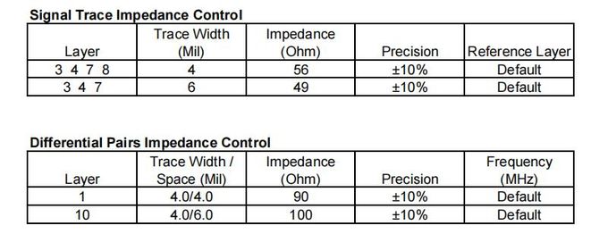
| Impedance Control | Single-Ended Trace Width: L3 / L4 / L7 / L8 --- 4mils --- 56 ohm, L3 / L4 / L 7 --- 6mils --- 49 ohm; Differential impedance: L1 --- 4 mils / 4 mils --- 90 ohm; L10 --- 4 mils / 6 mils --- 100 ohm |
| BOARD MATERIAL | |
| Glass Epoxy: | FR-4, ITEQ IT-180 TG>170, er<5.4 |
| Final foil external: | 1oz |
| Final foil internal: | 0.5oz |
| Final height of PCB: | 1.6mm ±0.16 |
| PLATING AND COATING | |
| Surface Finish | Immersion Gold (12.8%) 2µ"" over 100µ"" nickel |
| Solder Mask Apply To: | Top and Bottom, 12micon Minimum. |
| Solder Mask Color: | Green, PSR-2000GT600D, Taiyo supplied |
| Solder Mask Type: | LPSM |
| CONTOUR/CUTTING | Routing |
| MARKING | |
| Side of Component Legend | TOP and Bottom. |
| Colour of Component Legend | White, IJR-4000 MW300, Taiyo Supplied. |
| Manufacturer Name or Logo: | Marked on the board in a conductor and leged FREE AREA |
| VIA | Plated Through Hole(PTH), Blind via (L1-L4), buried via (L4-L6), Via in Pad and via tented and not be visible. |
| FLAMIBILITY RATING | UL 94-V0 Approval MIN. |
| DIMENSION TOLERANCE | |
| Outline dimension: | 0.0059"" (0.15mm) |
| Board plating: | 0.0030"" (0.076mm) |
| Drill tolerance: | 0.002"" (0.05mm) |
| TEST | 100% Electrical Test prior shipment |
| TYPE OF ARTWORK TO BE SUPPLIED | email file, Gerber RS-274-X, PCBDOC etc |
| SERVICE AREA | Worldwide, Globally. |