

 Home
-
Ceramic PCB
-
Al₂O₃ (96%) Ceramic PCB - 1.0mm Double-Sided Substrate with 1oz Copper and Immersion Gold for GBT Heat Dissipation
Home
-
Ceramic PCB
-
Al₂O₃ (96%) Ceramic PCB - 1.0mm Double-Sided Substrate with 1oz Copper and Immersion Gold for GBT Heat Dissipation
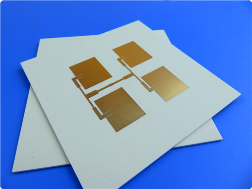
Al₂O₃ (96%) Ceramic PCB - 1.0mm Double-Sided Substrate with 1oz Copper and Immersion Gold for GBT Heat Dissipation
Printed Circuit Boards are custom-made products; the images and specifications provided are for reference only.
Brief Introduction
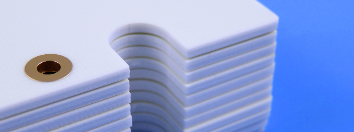
This Al₂O₃ ceramic PCB is constructed using high-grade 96% alumina (Al₂O₃) ceramic material, which delivers outstanding thermal conductivity, electrical insulation, and mechanical robustness. It adopts a 2-layer structure with a dielectric thickness of 1mm.
The double-sided 1oz copper cladding ensures excellent electrical conductivity and reliable signal transmission performance. The board has no solder mask or silkscreen markings applied. Its surface is finished with immersion gold—with a thickness of 2 micro-inches—providing strong solderability, oxidation resistance, and corrosion resistance.
This ceramic PCB is well-suited for electronic devices that demand high power, high frequency, and high reliability operation, such as IGBT modules requiring efficient heat dissipation.
Basic Specifications
Board dimensions: 98mm x 98mm=1PCS, +/- 0.15mm
Minimum Trace/Space: 6/6 mils
Minimum Hole Size: 0.3mm
No Blind vias.
Finished board thickness: 1.1mm
Finished Cu weight: 1oz (1.4 mils) outer layers
Via plating thickness: 20 μm
Surface finish: Immersion Gold
Top Silkscreen: No
Bottom Silkscreen: No
Top Solder Mask: No
Bottom Solder Mask: No
100% Electrical test used prior to shipment
PCB Specifications
| PCB SIZE | 98 x 98mm=1PCS |
| BOARD TYPE | |
| Number of Layers | Double sided Ceramic PCB |
| Surface Mount Components | YES |
| Through Hole Components | YES |
| LAYER STACKUP | copper ------- 35um(1oz) |
| 96% AL2O3 1.0mm | |
| copper ------- 35um(1oz) | |
| TECHNOLOGY | |
| Minimum Trace and Space: | 6mil/6mil |
| Minimum / Maximum Holes: | 0.3mm / 0.8mm |
| Number of Different Holes: | 7 |
| Number of Drill Holes: | 27 |
| Number of Milled Slots: | 0 |
| Number of Internal Cutouts: | 1 |
| Impedance Control | no |
| BOARD MATERIAL | |
| Glass Epoxy: | 96% AL2O3 1.0mm |
| Final foil external: | 1.0 oz |
| Final foil internal: | 0oz |
| Final height of PCB: | 1.1 mm ±0.1 |
| PLATING AND COATING | |
| Surface Finish | Immersion Gold |
| Solder Mask Apply To: | NO |
| Solder Mask Color: | NO |
| Solder Mask Type: | N/A |
| CONTOUR/CUTTING | Routing |
| MARKING | |
| Side of Component Legend | NO |
| Colour of Component Legend | NO |
| Manufacturer Name or Logo: | N/A |
| VIA | Plated Through Hole(PTH) |
| FLAMIBILITY RATING | 94 V-0 |
| DIMENSION TOLERANCE | |
| Outline dimension: | 0.0059"" (0.15mm) |
| Board plating: | 0.0030"" (0.076mm) |
| Drill tolerance: | 0.002"" (0.05mm) |
| TEST | 100% Electrical Test prior shipment |
| TYPE OF ARTWORK TO BE SUPPLIED | email file, Gerber RS-274-X, PCBDOC etc |
| SERVICE AREA | Worldwide, Globally. |
AL2O3 ZrO2 Data Sheet
| 1.Ceramic Parameters | 2. Material Thickness | |||||||||||
| Items | Unit | Al2O3 | ZTA | Ceramic Thickness | ||||||||
| Density | g/cm3 | ≥3.75 | ≥3.95 | 0.25mm | 0.32mm | 0.38mm | 0.50mm | 0.63mm | 1.0mm | |||
| Roughness (Ra) | μm | ≤0.6 | Ra≤0.6 | Copper Thickness | 0.15mm | ZTA | ZTA | Al2O3 | Al2O3 | Al2O3 | Al2O3 | |
| Bending strength | Mpa | ≥400 | ≥600 | 0.20mm | ZTA | ZTA | Al2O3 | Al2O3 | Al2O3 | Al2O3 | ||
| Coefficient of thermal expansion | 10^-6/K | ≤6.9 (40-400℃) | 7.5 (40-400℃) | 0.25mm | ZTA | ZTA | Al2O3 | Al2O3 | Al2O3 | Al2O3 | ||
| Thermal conductivity | W/(m*K) | ≥24 (25℃) | 26 (25℃) | 0.30mm | ZTA | ZTA | Al2O3 | Al2O3 | Al2O3 | Al2O3 | ||
| Dielectric constant | 1MHz | 9.8 | 10.2 | 0.40mm | ZTA | ZTA | - | - | - | - | ||
| Dielectric loss | 1MHz | 2*10^-4 | 2*10^-4 | |||||||||
| Volume resistivity | Ω*cm | >10^14 (25℃) | >10^14 (25℃) | |||||||||
| Dielectric strength | kV/mm | >15 | >15 |
Introduction of Al₂O₃ 96% Ceramic Material
The 96% purity alumina ceramic copper-clad laminate (CCL) is a high-performance electronic substrate material, composed of a 96% Al₂O₃ ceramic base and a high-purity copper layer laminated on its surface. The ceramic substrate is produced through a precision sintering process, while the copper layer is firmly bonded to the ceramic substrate using either Direct Bonded Copper (DBC) or Active Metal Brazing (AMB) technology—integrating excellent structural stability and functional versatility.
Key Characteristics
High Thermal Conductivity
The thermal conductivity of 96% alumina is approximately 24–28 W/(m·K), which enables efficient conduction of heat generated by high-power electronic devices. This performance is far superior to that of conventional PCB base materials.
Superior Electrical Insulation
The ceramic substrate features ultra-high resistivity (>10¹⁴ Ω·cm) and a breakdown voltage of 15–20 kV/mm, ensuring reliable insulation and long-term circuit safety in high-voltage applications.
Optimized Thermal Expansion Matching
The coefficient of thermal expansion (CTE) of 96% alumina is close to that of silicon chips (~7.1×10⁻⁶/℃), which minimizes thermal stress between the substrate and chips. This significantly reduces the risk of material failure or solder joint damage caused by temperature fluctuations.
Exceptional Mechanical & Thermal Durability
With a flexural strength of ≥300 MPa and a long-term operating temperature exceeding 800℃, this material can withstand harsh industrial environments (e.g., high temperatures, vibrations).
Balanced Cost-Effectiveness
Compared with 99% high-purity alumina, 96% alumina reduces raw material costs while retaining core performance characteristics. This makes it suitable for large-scale, cost-sensitive applications without compromising reliability.
Core Manufacturing Processes
Surface Metallization
DBC Process: The surface of alumina is oxidized to form an eutectic layer, which is then bonded to copper foil at high temperatures (above 1065℃) to achieve a strong, low-resistance interface.
AMB Process: Active solder is used to realize low-temperature brazing between the ceramic substrate and the copper layer, ensuring compatibility with temperature-sensitive components.
Precision Pattern Formation
Lithography and chemical etching techniques are applied to the copper layer to fabricate micro-scale circuits, meeting the requirements of high-density packaging and fine-pitch component integration.
Application Fields
Power Electronics
It is ideal for IGBT modules, new energy vehicle (NEV) motor controllers, and photovoltaic (PV) inverters. It enables efficient handling of high currents and rapid heat dissipation, ensuring the stable operation of power-dense devices.
LED Lighting
It is used as a Chip-on-Board (COB) substrate for high-power LEDs. Its excellent thermal conductivity improves heat dissipation efficiency, extending the lifespan of LED modules and preventing light degradation.
RF/Microwave Devices
It is applied in high-frequency circuits of 5G communication base stations and radar systems. With a low dielectric loss (tanδ<0.001), it minimizes signal attenuation and ensures high signal integrity in high-frequency scenarios.
Aerospace & Defense
Its high-temperature resistance and radiation resistance make it suitable for satellite power systems, avionics equipment, and other aerospace applications that require reliability in extreme environments.
Comparative Advantages
Versus AlN/Si₃N₄ Substrates: The 96% alumina ceramic CCL offers greater cost advantages and more mature manufacturing processes, making it a more accessible option for mainstream applications (compared to higher-cost aluminum nitride (AlN) or silicon nitride (Si₃N₄) substrates).
Versus Epoxy-Resin PCBs: It provides significantly improved heat resistance and thermal conductivity, enabling stable operation in scenarios with power densities exceeding 100 W/cm²—a capability that traditional epoxy-resin-based PCBs cannot achieve.
Development Trends
Driven by the miniaturization and increasing power density of electronic devices, 96% alumina ceramic materials are evolving in three key directions:
Ultra-Thin Substrates: Developing substrates with thicknesses below 0.2 mm to support compact device designs.
Multi-Layer & 3D Integration: Enabling multi-layer ceramic substrates and 3D structural designs to enhance circuit density and functional integration.
Performance Optimization: Improving thermo-mechanical properties through doping modification (e.g., adding trace elements to adjust CTE or thermal conductivity), expanding applications in emerging fields such as new energy storage and smart grids.
Our PCB processing Capability
We possess the capability to fabricate precision circuits with a minimum line width/space of 3mil/3mil, along with conductor thickness options ranging from 0.5oz to 14oz. Beyond standard circuit processing, we also offer advanced manufacturing capabilities, including micro-via filling, inorganic dam processing, and 3D circuit fabrication—catering to the complex requirements of high-end electronic applications.
In terms of substrate thickness, we can handle a wide range of specifications to meet diverse design needs, such as 0.25mm, 0.38mm, 0.5mm, 0.635mm, 1.0mm, 1.5mm, 2.0mm, 2.5mm, and 3.0mm.
To enhance the performance and reliability of PCBs, we provide diversified surface treatment solutions, including but not limited to the Electroplated Gold Process (with a thickness range of 1–30 μ"), the Electroless Nickel Palladium Immersion Gold (ENIG) Process (with a thickness range of 1–5 μ"), the Electroplated Silver Process (with a thickness range of 3–30 μm), the Electroplated Nickel Process (with a thickness range of 3–10 μm), and the Immersion Tin Process (with a thickness range of 1–3 μm).