

 Home
-
Ceramic PCB
-
AMB Si3N4 Ceramic PCB - 96% Ceramic Substrate High Thermal Conductivity 100μm Gold Plated Copper
Home
-
Ceramic PCB
-
AMB Si3N4 Ceramic PCB - 96% Ceramic Substrate High Thermal Conductivity 100μm Gold Plated Copper
AMB Si3N4 Ceramic PCB - 96% Ceramic Substrate High Thermal Conductivity 100μm Gold Plated Copper
Printed Circuit Boards are custom-made products; the images and specifications provided are for reference only.
Brief Introduction
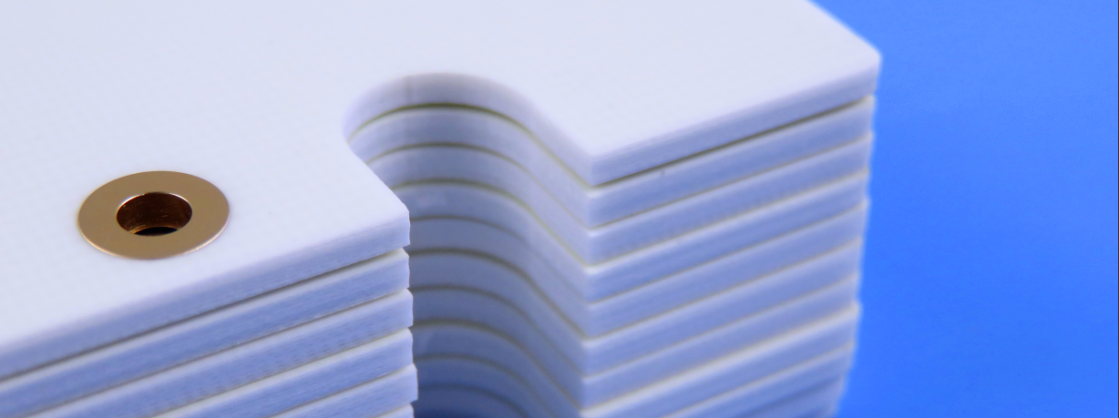
This single-sided ceramic PCB features a 96% silicon nitride (Si₃N₄) ceramic substrate, utilizing Active Metal Brazing (AMB) technology for superior bonding performance. The AMB-Si₃N₄ ceramic circuit board combines key advantages: high thermal conductivity (80 W/m·K), excellent electrical insulation, high heat capacity, and a thermal expansion coefficient that closely matches chip materials—minimizing thermal stress during operation.
Equipped with 100μm (2.85oz) heavy copper, the board ensures efficient current conduction, making it suitable for high-power applications. Its surface is finished with thick gold plating, which not only provides a reliable bonding interface for component mounting but also enhances oxidation resistance and wear durability, extending the PCB's service life.
Designed without solder mask or silkscreen, this PCB offers maximum flexibility to accommodate custom soldering processes and specific application needs. All units are manufactured in compliance with IPC Class 2 standards, ensuring consistent quality and performance reliability.
Basic Specifications
PCB size: 42mm x 41mm=1PCS
Layer count: single sided ceramic PCB
Thickness:0.25mm
Base material: 96% Si3N4 Ceramic Substrates
Surface finish: Gold plated
Thermal conductivity of dielectric: 80 W/MK
Copper weight: 100um (2.85oz)
Gold thickness: >=1um (39.37 micro-inch)
No solder mask or silkscreen
Technology: Active Metal Brazing (AMB)
Basic Specifications
| PCB SIZE | 42 x 41mm=1PCS |
| BOARD TYPE | |
| Number of Layers | Double sided Ceramic PCB |
| Surface Mount Components | YES |
| Through Hole Components | N/A |
| LAYER STACKUP | copper ------- 100um(2.85oz) |
| Si3N4 Ceramic -0.25mm | |
| copper ------- 100um(2.85oz) | |
| TECHNOLOGY | |
| Minimum Trace and Space: | 25mil / 25mil |
| Minimum / Maximum Holes: | 0.5mm / 1.0mm |
| Number of Different Holes: | 2 |
| Number of Drill Holes: | 2 |
| Number of Milled Slots: | 0 |
| Number of Internal Cutouts: | 1 |
| Impedance Control | no |
| BOARD MATERIAL | |
| Glass Epoxy: | Si3N4 Ceramic -0.25mm |
| Final foil external: | 2.85 oz |
| Final foil internal: | N/A |
| Final height of PCB: | 0.3 mm ±0.1mm |
| PLATING AND COATING | |
| Surface Finish | Electroplated Gold (hard gold) |
| Solder Mask Apply To: | NO |
| Solder Mask Color: | NO |
| Solder Mask Type: | N/A |
| CONTOUR/CUTTING | Routing |
| MARKING | |
| Side of Component Legend | NO |
| Colour of Component Legend | NO |
| Manufacturer Name or Logo: | N/A |
| VIA | Non Plated Through Hole(NPTH) |
| FLAMIBILITY RATING | 94 V-0 |
| DIMENSION TOLERANCE | |
| Outline dimension: | 0.0059"" (0.15mm) |
| Board plating: | 0.0030"" (0.076mm) |
| Drill tolerance: | 0.002"" (0.05mm) |
| TEST | 100% Electrical Test prior shipment |
| TYPE OF ARTWORK TO BE SUPPLIED | email file, Gerber RS-274-X, PCBDOC etc |
| SERVICE AREA | Worldwide, Globally. |
.png)
Data Sheets
| 1.Ceramic Parameters | 2. Material Thickness | ||||||||||
| Items | Unit | Al2O3 | Si3N4 | Copper Thickness | |||||||
| Density | g/cm3 | ≥3.3 | ≥3.22 | 0.15mm | 0.25mm | 0.30mm | 0.50mm | 0.8mm | |||
| Roughness (Ra) | μm | ≤0.6 | ≤0.7 | Ceramic Thickness | 0.25mm | Si3N4 | Si3N4 | Si3N4 | Si3N4 | - | |
| Bending strength | Mpa | ≥450 | ≥700 | 0.32mm | Si3N4 | Si3N4 | Si3N4 | Si3N4 | Si3N4 | ||
| Coefficient of thermal expansion | 10^-6/K | 4.6~5.2 (40-400℃) | 2.5~3.1 (40-400℃) | 0.38mm | AlN | AlN | AlN | - | - | ||
| Thermal conductivity | W/(m*K) | ≥170 (25℃) | 80 (25℃) | 0.50mm | AlN | AlN | AlN | - | - | ||
| Dielectric constant | 1MHz | 9 | 9 | 0.63mm | AlN | AlN | AlN | - | - | ||
| Dielectric loss | 1MHz | 2*10^-4 | 2*10^-4 | 1.00mm | AlN | AlN | AlN | - | - | ||
| Volume resistivity | Ω*cm | >10^14 (25℃) | >10^14 (25℃) | ||||||||
| Dielectric strength | kV/mm | >20 | >15 |
Active Metal Brazing (AMB) Technology
The AMB (Active Metal Brazing) process is a method that utilizes a small amount of active elements (e.g., titanium, Ti) contained in the brazing filler metal. These elements react with the ceramic surface to generate a reaction layer, which enables wetting and soldering by the liquid brazing filler metal—thus achieving a stable bond between ceramic and metal components.
Si₃N₄ (Silicon Nitride) Ceramic Substrates
Si₃N₄ ceramic substrates are advanced materials renowned for their exceptional mechanical, thermal, and electrical properties, making them ideal for high-performance applications across industries.
These ceramic substrates offer full customization to meet specific customer requirements, including tailored ceramic thickness, copper layer thickness, and surface treatment options.
Their low coefficient of thermal expansion (CTE) ranges from 2.5 to 3.1 ppm/K (40-400°C), which closely matches that of silicon and other semiconductor materials. This minimizes thermal stress in electronic devices, ensuring long-term operational stability. With a thermal conductivity of 80 W/(m·K) at 25°C, they enable efficient heat dissipation, making them suitable for high-power and high-temperature operating environments.
Si₃N₄ ceramics boast an impressive bending strength of ≥700 MPa, providing exceptional mechanical durability for demanding applications. They support the brazing of copper layers thicker than 0.8mm, which reduces thermal resistance and enables the handling of high current loads. Additionally, these substrates feature selective Ag plating and sintered Ag processes, ensuring perfect compatibility with SiC chips for optimal performance.
Our PCB Processing Capability
We can process precision circuits with a line width/space of 3mil/3mil and a conductor thickness ranging from 0.5oz to 14oz. We also possess advanced processing capabilities, including micro-via filling, inorganic dam processing, and 3D circuit fabrication, to address complex design requirements.
We can handle a variety of substrate thicknesses, such as 0.25mm, 0.38mm, 0.5mm, 0.635mm, 1.0mm, 1.5mm, 2.0mm, 2.5mm, and 3.0mm, to diverse application scenarios.
We offer diversified surface treatment solutions, including the Electroplated Gold Process (1-30u"), Electroless Nickel Palladium Immersion Gold Process (1-5u"), Electroplated Silver Process (3-30μm), Electroplated Nickel Process (3-10μm), and Immersion Tin Process (1-3μm), to enhance PCB performance and reliability.