| |
|
|
|
|
|
|
|
|
| |
|
| F4B PCB |
| |
|
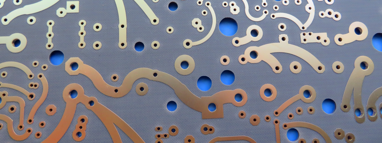
F4B is a high-frequency material produced by Taizhou Wangling Insulation Materials Factory. It primarily uses PTFE as the substrate, filled with fiberglass cloth and nano-level ceramic film. F4B PCBs are designed for applications that require excellent electrical performance, particularly in microwave and RF circuits. F4B PCBs offer low dielectric loss, high thermal stability, and superior chemical resistance, making them suitable for demanding environments. The F4B material possesses unique properties that significantly reduce signal degradation, which is essential for high-speed data transmission. This characteristic ensures that signals maintain their integrity over long distances and through complex circuit paths. Furthermore, F4B PCBs are capable of accommodating intricate circuit designs, allowing engineers to develop compact and efficient layouts that optimize space and performance. As a result, these PCBs are extensively utilized in various industries, including telecommunications, aerospace, and automotive. |
|
|
.JPG) |
| Double Sided F4BME265 High Frequency PCB DK2.65 PTFE with OSP and Green Mask |
The PCB being discussed is 89mm x 61mm, one per panel. It's a double-sided PCB with two conductive layers for circuitry. It has through-hole components, not surface-mount ones. The layer stack-up begins with a 35um (1oz) copper layer. In the middle is 1.5mm thick F4BME265 material. After plating, there's another 35um (1oz) copper layer on the opposite side. |
Tags:
| F4B High-frequency Material |
F4B F4BME265 Substrate |
F4BME Series Laminates |
PTFE RF PCB 1.5mm Thickness |
F4BME265 High-frequency PCB |
|
|
| |
|
.jpg) |
| 1.5mm F4BTM350 PTFE High Frequency PCB Board with 3oz Copper and Immersion Silver |
| This is a double-sided PCB on F4BTM350 high-frequency substrates, sized 67mm x 85mm with top surface mount components. The layer stackup combines 3oz copper and F4BTM350 dielectric for excellent electrical conductivity and thermal management. Finished with immersion silver and a green solder mask on top for solderability, surface protection, aesthetic appeal, and durability. |
Tags:
F4BTM Series Laminates |
Wangling F4BTM350 Substrate |
1.5mm F4BTM350 High Frequency PCB |
2-Layer Low Dissipation PCB |
PTFE Plate F4BTM350 PCB |
|
|
| |
|
 |
| Wangling F4BM265 PCB DK 2.65 PTFE Material with 3oz Copper Immersion Gold Top Choice for RF Circuit Boards |
| This board is designed as a double-sided PCB, utilizing F4BM265 as the substrate with a DK value of 2.65. It measures 210mm in length and 115mm in width, with a finished thickness of 1.6mm. The board features a 3oz finished copper weight, and it comes without solder mask or silkscreen. The surface finish is immersion gold. |
Tags:
F4BM265 RF Circuit Board |
F4BM265 High Frequency PCB |
3oz Copper Coating PCB |
F4BM265 PTFE PCB |
DK 2.65 F4BM265 Substrate |
|
|
| |
|
 |
| 3.0mm Double Layer F4BTME300 High-Frequency PCB PTFE RF Board with Immersion Silver Optimized for RF Applications |
| F4BTME300 High Frequency PCB measures 170 mm x 95 mm and is designed as a double-sided, two-layer board. It supports surface-mount components but does not accommodate through-hole components in this configuration. The stack-up includes a top layer with 35 µm (1 oz) copper, starting with a 0.5 oz base plating, paired with a 3.0 mm thick F4BTME300 core material. The bottom layer also features 35 µm (1 oz) copper with plating. The board utilizes immersion silver for superior solderability and protection. |
Tags:
F4BTME300 PCB |
F4BTME Series Substrate |
F4BTME300 3.0mm PCB |
F4BTME300 Material |
F4BTME300 RF PCB |
|
|
| |
|
.PNG) |
| F4BM220 High-Frequency PCB 3.0mm PTFE DK 2.2 with 1oz Copper HASL Lead-Free for Superior Signal Integrity |
This board is designed as a double-sided PCB, utilizing F4BM220 as the substrate with a dielectric constant (DK) of 2.2. It measures 61mm in length and 62mm in width, with a finished thickness of 3.0mm. Wangling F4BM220 PCB features a 1.0oz finished copper weight and comes without solder mask or silkscreen. The surface finish is OSP (Organic Solderability Preservative). |
Tags:
F4BM220 High Frequency PCB |
3.0mm F4BM220 PCB |
F4BM220 Printed Circuit Board |
F4BM Series Laminates |
F4BM PTFE PCB |
|
|
| |
|
 |
| Metal Based RF PCB with Aluminum or Copper Base with Immersion Gold for Shielding and Heat Dissipation |
| Metal-based substrates are innovative composites designed for high-frequency applications. These substrates feature a core of high-frequency materials such as PTFE, sandwiched between specialized layers. On one side, a copper foil layer is applied, while the opposite side is coated with either a copper or aluminum base. This unique structure provides exceptional shielding and heat dissipation capabilities, making it ideal for demanding electronic environments. |
Tags:
F4B Aluminum / Copper Base PCB |
F4BM and F4BME series aluminum/copper substrates |
F4BTM and F4BTME series aluminum/copper substrates |
F4BTMS series aluminum/copper substrates |
Metal-based substrates |
|
|
| |
|
陔.jpg) |
| 0.8mm F4BTMS265 High-Frequency PCB 1oz Copper Immersion Gold Black Solder Mask for Satellite Communications from Wangling |
| Wangling F4BTMS265 PCB features a 2-layer copper design and is exclusively equipped with surface mount components. The board dimensions are 120mm x 65mm, with 1 piece per panel. It begins with a 17μm (0.5 oz) copper base, which is plated on both the top and bottom layers. The core material, F4BTMS265, has a thickness of 0.762mm and is positioned centrally. The surface finish is immersion gold, and the top layer is coated with a black solder mask. |
Tags:
Wangling F4BTMS Datasheet |
0.8mm F4BTMS265 High Frequency PCB |
F4BTMS265 PCB Price |
F4BTMS265 Black Solder Mask |
2-layer F4BTMS265 Substrate |
|
|
| |
|
.jpg) |
| 1.0mm 2-layer F4BTME320 PCB 2oz Copper Immersion Gold Offering Enhanced Durability and Aesthetics |
| This is a 2-layer high-frequency printed circuit board (PCB) constructed using Wangling F4BTME320 substrates. Both the top and bottom layers are built with 70 µm (2 oz) copper, starting from a base of 1 oz plating. The design supports surface mount components exclusively on the top side, with no through-hole components incorporated. Key technical specifications include a minimum trace width of 4 mil and a minimum spacing of 6 mil, enabling high-precision circuit layout. |
Tags:
F4BTME320 High-Frequency PCB |
Wangling F4BTME Datasheet |
F4BTME320 2oz Copper |
F4BTME320 Immersion-Gold PCB |
2-layer F4BTME320 Laminate |
|
|
| |
|
.jpg) |
| DK6.15 F4BTMS615 PCB 1.6mm F4B Substrate with Low CTE and Immersion Gold Ideal for Aerospace Applications |
| F4BTMS615 PCB is designed with two copper layers and features a compact dimensions of 171 mm x 58 mm. It accommodates surface mount components exclusively on the top layer. The layer stackup includes a top layer with 35 µm (1 oz) copper, starting from a base of 0.5 oz plating, and is supported by a robust F4BTMS615 core material with a thickness of 1.524 mm at its center. |
Tags:
Wangling F4BTMS615 PCB |
F4BTMS Series High Frequency Laminates |
DK6.15 F4BTMS615 PCB |
F4BTMS Series Laminates |
F4BTMS615 Dual Layer PCB |
|
|
| |
|
.jpg) |
| F4BTM320 PCB 2oz Copper 1.27mm Substrates with Immersion Gold Ensuring Excellent Solderability and Durability |
| F4BTM320 PCB measures 110mm x 76mm and is designed as a double-sided board with two copper layers. It supports surface mount components exclusively, with no through-hole components included. The layer stackup consists of a top layer with 70 µm (2 oz) copper, starting from a base of 1 oz plating, reinforced by a durable F4BTM320 core material with a thickness of 1.27mm. The bottom layer mirrors the same copper specifications to ensure uniform performance. |
Tags:
Wangling F4BTM320 PCB |
F4BTM Series PCB |
2oz Copper F4B PCB |
F4BTM320 High Frequency PCB |
2-layer F4BTM320 Substrate |
|
|
| |
|
| |
|
| |
|
|
|
|
|
|
|
|
|
|