| |
|
|
|
|
|
|
|
|
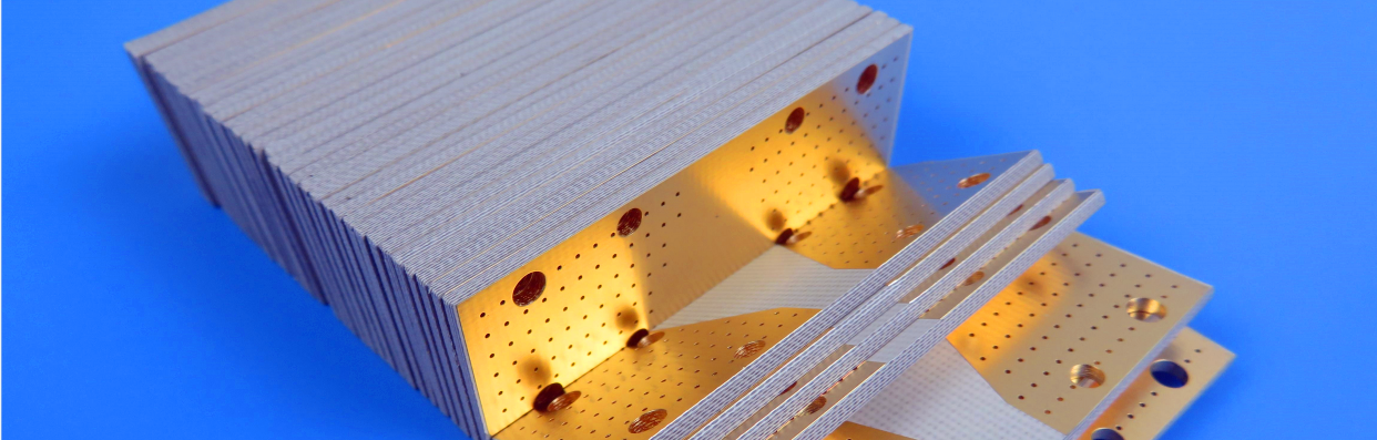
F4BTM320 PCB 2oz Copper 1.27mm Substrates with Immersion Gold Ensuring Excellent Solderability and Durability |
|
|
(Printed Circuit Boards are custom-made products. The picture and parameters shown are for reference only.) |
|
|
|
|
|
Brief Introduction |
|
|
F4BTM320 PCB measures 110mm x 76mm and is designed as a double-sided board with two copper layers. It supports surface mount components exclusively, with no through-hole components included. The layer stackup consists of a top layer with 70 µm (2 oz) copper, starting from a base of 1 oz plating, reinforced by a durable F4BTM320 core material with a thickness of 1.27mm. The bottom layer mirrors the same copper specifications to ensure uniform performance.
The design allows for a minimum trace width of 5 mil and a minimum spacing of 9 mil, enabling high-precision circuit layout. The surface finish is immersion gold, which enhances solderability and provides long-lasting durability. Both the top and bottom sides are coated with a black solder mask for protection and a sleek appearance, while the top side also features white silkscreen for clear labeling and component identification.
Additional details are provided in the table below. |
|
|
|
|
|
Basic specifications |
|
|
F4BTM320 High Frequency PCB 2oz Copper 1.27mm Substrates With Immersion Gold |
|
|
PCB SIZE |
110mm x 76 mm =1up |
BOARD TYPE |
Double sided PCB |
Number of Layers |
2 layers |
Surface Mount Components |
YES |
Through Hole Components |
NO |
LAYER STACKUP |
copper ------- 70 um(1 oz+plate) TOP layer |
|
F4BTM320 - 1.27mm |
|
copper ------- 70 um(1 oz + plate) BOT Layer |
TECHNOLOGY |
|
Minimum Trace and Space: |
5 mil / 9 mil |
Minimum / Maximum Holes: |
0.35 mm / 1.0 mm |
Number of Different Holes: |
4 |
Number of Drill Holes: |
61 |
Number of Milled Slots: |
0 |
Number of Internal Cutouts: |
0 |
Impedance Control: |
no |
Number of Gold finger: |
0 |
BOARD MATERIAL |
|
Glass Epoxy: |
F4BTM320 DK3.2 |
Final foil external: |
2 oz |
Final foil internal: |
N/A |
Final height of PCB: |
1.4 mm |
PLATING AND COATING |
|
Surface Finish |
Immersion Gold |
Solder Mask Apply To: |
Top side & Bottom Side |
Solder Mask Color: |
Black |
Solder Mask Type: |
N/A |
CONTOUR/CUTTING |
Routing |
MARKING |
|
Side of Component Legend |
Top Side |
Colour of Component Legend |
White |
Manufacturer Name or Logo: |
N/A |
VIA |
Plated through hole(PTH), minimum size 0.35mm. |
FLAMIBILITY RATING |
UL 94-V0 Approval MIN. |
DIMENSION TOLERANCE |
|
Outline dimension: |
0.0059" |
Board plating: |
0.0029" |
Drill tolerance: |
0.002" |
TEST |
100% Electrical Test prior shipment |
TYPE OF ARTWORK TO BE SUPPLIED |
email file, Gerber RS-274-X, PCBDOC etc |
SERVICE AREA |
Worldwide, Globally. |
|
|
|
|
|
|
.jpg) |
|
|
|
|
|
F4BTM High Frequency Laminates |
|
|
The F4BTM series laminates are manufactured through a scientifically optimized blend of fiberglass cloth, nano-ceramic fillers, and polytetrafluoroethylene resin, processed under stringent pressing conditions. This series is built on the F4BM dielectric layer and enhanced with high-dielectric, low-loss nano-ceramics, delivering a higher dielectric constant, superior heat resistance, a reduced thermal expansion coefficient, increased insulation resistance, and improved thermal conductivity, all while retaining its low-loss properties. The laminates offer optional ED copper foil in thicknesses of 0.5 oz, 1 oz, 1.5 oz, and 2 oz to meet diverse design requirements. |
|
|
|
|
|
Features and Benefits |
|
|
DK 2.98-3.5 optional
Adding ceramic improves performance
Excellent PIM indicators
Rich thickness ranging 0.254mm to 12mm
Diversified size 460mm x 610mm to 914mm x 1220mm
Cost saving
Commercialization for mass production
High cost performance
Anti radiation
Low exhaust |
|
|
|
|
|
Our PCB Capability (F4BTM) |
|
|
PCB Capability (F4BTM) |
PCB Material: |
PTFE / glass fiber cloth / Nano-ceramic filler |
Designation (F4BTM ) |
F4BTM |
DK (10GHz) |
DF (10 GHz) |
|
F4BTM298 |
2.98±0.06 |
0.0018 |
|
F4BTM300 |
3.0±0.06 |
0.0018 |
|
F4BTM320 |
3.2±0.06 |
0.0020 |
|
F4BTM350 |
3.5±0.07 |
0.0025 |
Layer count: |
Single Sided, Double Sided PCB, Multilayer PCB, Hybrid PCB |
Copper weight: |
0.5oz (17 µm), 1oz (35µm), 2oz (70µm) |
Dielectric thickness (or overall thickness) |
0.25mm, 0.508mm, 0.762mm, 0.8mm, 1.0mm, 1.016mm, 1.27mm, 1.524mm, 2.0mm, 3.0mm, 4.0mm, 5.0mm, 6.0mm, 8.0mm, 10.0mm, 12.0mm |
PCB size: |
≤400mm X 500mm |
Solder mask: |
Green, Black, Blue, Yellow, Red etc. |
Surface finish: |
Bare copper, HASL, ENIG, Immersion silver, Immersion tin, OSP, Pure gold, ENEPIG etc.. |
|
|
|
|
|
|
Data Sheet (F4BTM) |
|
|
Product Technical Parameters |
Product Models & Data Sheet |
Product Features |
Test Conditions |
Unit |
F4BTM298 |
F4BTM300 |
F4BTM320 |
F4BTM350 |
Dielectric Constant (Typical) |
10GHz |
/ |
2.98 |
3.0 |
3.2 |
3.5 |
Dielectric Constant Tolerance |
/ |
/ |
±0.06 |
±0.06 |
±0.06 |
±0.07 |
Loss Tangent (Typical) |
10GHz |
/ |
0.0018 |
0.0018 |
0.0020 |
0.0025 |
|
20GHz |
/ |
0.0023 |
0.0023 |
0.0026 |
0.0035 |
Dielectric Constant Temperature Coefficient |
-55 º~150ºC |
PPM/℃ |
-78 |
-75 |
-75 |
-60 |
Peel Strength |
1 OZ F4BTM |
N/mm |
>1.6 |
>1.6 |
>1.6 |
>1.6 |
|
1 OZ F4BTME |
N/mm |
>1.4 |
>1.4 |
>1.4 |
>1.4 |
Volume Resistivity |
Standard Condition |
MΩ.cm |
≥1×10^7 |
≥1×10^7 |
≥1×10^7 |
≥1×10^7 |
Surface Resistivity |
Standard Condition |
MΩ |
≥1×10^6 |
≥1×10^6 |
≥1×10^6 |
≥1×10^6 |
Electrical Strength (Z direction) |
5KW,500V/s |
KV/mm |
>26 |
>30 |
>32 |
>32 |
Breakdown Voltage (XY direction) |
5KW,500V/s |
KV |
>34 |
>35 |
>40 |
>40 |
Coefficientof Thermal Expansion |
XY direction |
-55 º~288ºC |
ppm/ºC |
15,16 |
15,16 |
13,15 |
10,12 |
|
Z direction |
-55 º~288ºC |
ppm/ºC |
78 |
72 |
58 |
51 |
Thermal Stress |
260℃, 10s,3 times |
No delamination |
No delamination |
No delamination |
No delamination |
Water Absorption |
20±2℃, 24 hours |
% |
≤0.05 |
≤0.05 |
≤0.05 |
≤0.05 |
Density |
Room Temperature |
g/cm3 |
2.25 |
2.25 |
2.20 |
2.20 |
Long-Term Operating Temperature |
High-Low Temperature Chamber |
℃ |
-55~+260 |
-55~+260 |
-55~+260 |
-55~+260 |
Thermal Conductivity |
Z direction |
W/(M.K) |
0.42 |
0.42 |
0.50 |
0.54 |
PIM |
Only applicable to F4BTME |
dBc |
≤-160 |
≤-160 |
≤-160 |
≤-160 |
Flammability |
/ |
UL-94 |
V-0 |
V-0 |
V-0 |
V-0 |
Material Composition |
/ |
/ |
PTFE, Fiberglass Cloth, nano-ceramics
F4BTM paired with ED copper foil, F4BTME paired with reverse-treated (RTF) copper foil. |
|
|
|
|
|
|
|
|
|
|
|
|
Hot Tags:
Wangling F4BTM320 PCB |
F4BTM Series PCB |
2oz Copper F4B PCB |
F4BTM320 High Frequency PCB |
2-layer F4BTM320 Substrate |
|
|
|