|
|
|
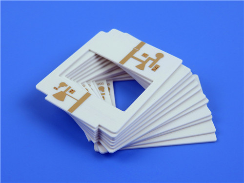
TMM10i PCB 25mil 2-Layer Pure Gold RF Board Optimized for 5G Microstrip Antenna From Rogers |
|
|
|
|
|
|
|
1. Introduction of TMM10i PCB
Rogers TMM10i ceramic-thermoset composite PCBs deliver isotropic dielectric stability (Dk 9.8±0.045) across 1-40GHz frequencies, engineered for mission-critical stripline/microstrip designs in radar and satellite communications.Rogers TMM10i PCB hybrid material combines PTFE-grade electrical performance with FR-4-like processability, achieving 100% plated through-hole (PTH) reliability under MIL-STD-202G thermal shock testing (-55°C to +125°C).
Unlike conventional ceramic substrates, TMM10i PCB’s polymer-ceramic matrix enables 30% faster prototyping through standard PCB etching drills, while its 0.0025 dissipation factor minimizes insertion loss in 28GHz mmWave beamforming arrays. The copper-matched CTE (13/17/50 ppm/°C) TMM10i laminate prevents solder joint fatigue in high-power GaN amplifiers, outperforming RO4003C in thermal cycling endurance by 2.5X. |
|
2. Features
- Dk of 9.80 +/- .245
- Dissipation factor of .0020 at 10GHz
- Thermal coefficient of Dk of -43 ppm/°K
- Coefficient of thermal expansion matched to copper
- Decomposition Temperature (Td) of 425 °C TGA
- Coefficient of Thermal Expansion - x y z : 19ppm/K, 19ppm/K,20ppm/K
- Thermal Conductivity of 0.76W/mk
- Available in a thickness range of .0015 to .500 inches +/- .0015” |
|
|
|
3. Benefits
- Mechanical properties resist creep and cold flow
- Resistant to process chemicals, reducing damage during fabrication
- Material does not require a sodium napthanate treatment prior to electroless plating
- Based on a thermoset resin, allowing for reliable wire-bonding
- Reliable wirebonding |
|
|
|
4. PCB Stackup: 2-layer rigid PCB
Copper_layer_1 - 35 μm
Rogers TMM10i Core - 0.635 mm (25mil)
Copper_layer_2 - 35 μm |
|
|
|
| 5. PCB Construction Details: |
| |
| - Base material: TMM10i
- Layer count: Double sided
- Board dimensions: 91mm x 91 mm=1PCS, +/- 0.15mm
- Minimum Trace/Space: 5/5 mils
- Minimum Hole Size: 0.3mm
- No Blind vias.
- Finished board thickness: 0.7mm
- Finished Cu weight: 1oz (1.4 mils) outer layers
- Via plating thickness: 20 μm
- Surface finish: Pure gold (No nickle under gold)
- Top Silkscreen: No
- Bottom Silkscreen: No
- Top Solder Mask: No
- Bottom Solder Mask: No
- 100% Electrical test used prior to shipment |
| |
|
 |
|
|
6. PCB Statistics:
Components: 15
Total Pads: 33
Thru Hole Pads: 21
Top SMT Pads: 12
Bottom SMT Pads: 0
Vias: 42
Nets: 2
|
|
|
|
7. Type of artwork supplied: Gerber RS-274-X |
|
|
|
8. Quality standard: IPC-Class-2 |
|
|
|
9. Availability: worldwide |
|
|
|
10. Typical Applications:
- RF and microwave circuitry
- Power amplifiers and combiners
- Filters and coupler
- Satellite communication systems
- Global Positioning Systems Antennas
- Patch Antennas
- Dielectric polarizers and lenses
- Chip testers |
|
|
|
|
|
|
|
|
|
|
|
|
|
NEXT: TP980 7.62mm ENIG PCB 2-Layer Dk3-25 Adjustable Ceramic/PPO RF Substrate in Aerospace Telemetry Systems |
|
|
|
|
|
|