|
|
|
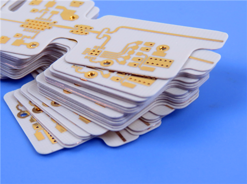
TFA300 High Frequency PCB 2-Layer 10mil PTFE Ceramic PCB Aerospace Grade RF Substrate with Dk3.0 |
|
|
|
|
|
|
|
1. Introduction of TFA series PCB
The TFA series redefines RF/microwave circuit performance through its glass-free PTFE-ceramic composite structure, engineered to eliminate electromagnetic interference from traditional fiberglass substrates. Utilizing nano-ceramic particle infusion technology, TFA laminates deliver isotropic dielectric properties (Dk tolerance ±0.05) across X/Y/Z axes, achieving 0.0018 dielectric loss at 40GHz for 5G mmWave and satellite communication systems. With CTE values matching copper foil (13/17/50 ppm/°C), they prevent solder joint fatigue in high-power GaN amplifiers operating from -65°C to +150°C.
Four standardized Dk options (2.94/3.0/6.15/10.2)—categorized as TFA294, TFA300, TFA615, TFA1020—enable precise impedance control for phased array radars and aerospace telemetry systems. The proprietary lamination process enhances thermal conductivity (0.71 W/m·K), reducing hotspot temperatures by 40% compared to conventional FR-4/Rogers hybrids. As a direct replacement for imported RO3003/RO3010 substrates, TFA series PCB cuts procurement lead times by 6-8 weeks while meeting MIL-PRF-55110G specifications.
|
|
2. Features of TFA300 PCB: |
|
- Dielectric constant (Dk) of 3.0±0.04 at 10GHz
- Dissipation factor of .001 at 10GHz and 20 GHz, 0.0012 at 40 GHz
- Low TCDK at -8 ppm/°C, -55°C to 150°C
- CTE x-axis of 18 ppm/°C, CTE y-axis of 18 ppm/°C, CTE z-axis of 30 ppm/°C, -55°C to 288°C
- Thermal conductivity of 0.6 W/mk
- Moisture absorption of 0.04%
- UL 94-V0 |
|
|
|
3. PCB Stack-up: 2-layer Rigid PCB
Copper_layer_1 - 35 μm
TFA300 Core - 0.254 mm (10mil)
Copper_layer_2 - 35 μm
|
|
|
|
| 4. PCB Construction details: |
| |
| - Base material: TFA300
- Layer count: 2 layers
- Board dimensions: 65mm x 51 mm=1PCS, +/- 0.15mm
- Minimum Trace/Space: 5/7 mils
- Minimum Hole Size: 0.3mm
- No Blind vias.
- Finished board thickness: 0.3mm
- Finished Cu weight: 1oz (1.4 mils) outer layers
- Via plating thickness: 20 μm
- Surface finish: Immersion Gold
- Top Silkscreen: No
- Bottom Silkscreen: No
- Top Solder Mask: No
- Bottom Solder Mask: No
- 100% Electrical test used prior to shipment |
| |
|
 |
| |
|
|
|
5. PCB Statistics:
Components: 12
Total Pads: 43
Thru Hole Pads: 27
Top SMT Pads: 16
Bottom SMT Pads: 0
Vias: 11
Nets: 2
|
|
|
|
6. Type of artwork supplied: Gerber RS-274-X |
|
|
|
7. Quality standard: IPC-Class-2 |
|
|
|
8. Availability: worldwide |
|
|
|
9. Some Typical Applications:
- Aerospace equipment, space, in-cabin equipment, aircraft;
- Microwaves, antennas, phase-sensitive antennas;
- Early warning radars, airborne radars, etc.;
- Phased array antennas, beamforming networks;
- Satellite communications, navigation;
- Power amplifiers. |
|
|
|
|
|
|
|
|
|
|
|
|
|
NEXT: TMM10i PCB 25mil 2-Layer Pure Gold RF Board Optimized for 5G Microstrip Antenna From Rogers |
|
|
|
|
|
|