|
|
|
Rogers RO4360G2 2-Layer 8mil Circuit Board Superior RF Laminate with Enhanced Rigidity and Lead-Free Processing |
|
|
|
|
|
|
|
1. Introduction of RO4360G2 PCB
RO4360G2 laminates are high-performance, low-loss RF materials featuring a unique ceramic-filled, glass-reinforced thermoset construction that delivers exceptional electrical properties while maintaining FR-4-like processability. As the first high-Dk thermoset laminate compatible with standard PCB fabrication methods, RO4360G2 PCB offers superior rigidity for enhanced multilayer board processing, lead-free manufacturing compatibility, and significant cost savings versus traditional high-frequency materials. RO4360G2 versatile laminates can be seamlessly combined with RO4400 series prepregs and lower-Dk RO4000 laminates, providing designers with flexible, cost-effective solutions for demanding RF and microwave applications without compromising performance or manufacturability.
|
|
2. Features
- Dielectric constant of 6.15+/- 0.15 at 10 GHz/23°C
- Dissipation factor of 0.0038 at 10 GHz/23°C
- Td> 407°C, High Tg greater than 280 °C TMA
- High Thermal Conductivity of 0.75 W/mK
- Low Z-axis coefficient of thermal expansion at 28 ppm/°C
- Copper matached Coefficient of Thermal Expansion (-55 to 288 °C)£ºX axis 13 ppm/°C, Y axis 14 ppm/°C
- Lead free Process Compatible, 94V-0 flammability. |
|
|
|
3. Benefits
-Design flexibility
-Plated through-hole reliability
-Automated assembly compatible
-Environmentally friendly- Lead free process compatible
-Efficient supply chain and short lead times reduce overall project costs |
|
|
|
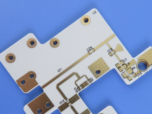
4. PCB Stackup: 2-layer rigid PCB
Copper_layer_1 - 35 μm
Rogers RO4360G2 Substrate - 8mil (0.203mm)
Copper_layer_2 - 35 μm |
|
| 5. PCB Construction Details: |
| |
| - Base material: RO4360G2
- Layer count: 2 layers
- Board dimensions: 76.32mm x 67.51 mm=1PCS
- Minimum Trace/Space: 4/6 mils
- Minimum Hole Size: 0.20mm
- No Blind vias.
- Finished board thickness: 0.3mm
- Finished Cu weight: 1 oz (1.4 mils) outer layers
- Via plating thickness: 20 μm
- Surface finish: Electroless Nickel Immersion Gold (ENIG)
- Top Silkscreen: No
- Bottom Silkscreen: No
- Top Solder Mask: No
- Bottom Solder Mask: No
- 100% Electrical test used prior to shipment |
| |
|
 |
|
|
6. PCB Statistics:
Components: 18
Total Pads: 57
Thru Hole Pads: 39
Top SMT Pads: 18
Bottom SMT Pads: 0
Vias: 51
Nets: 2
|
|
|
|
7. Type of artwork supplied: Gerber RS-274-X |
|
|
|
8. Quality standard: IPC-Class-2 |
|
|
|
9. Availability: worldwide |
|
|
|
10. Typical Applications:
- Base Station Power Amplifiers
- Small Cell Transceivers |
|
|
|
|
|
|
|
|
|
|
|
|
|
NEXT: RTduroid 5880 2-Layer 20mil Immersion Gold PCB Low Loss PTFE Composite for Stripline and Microstrip Circuit Applications |
|
|
|
|
|
|