|
|
|
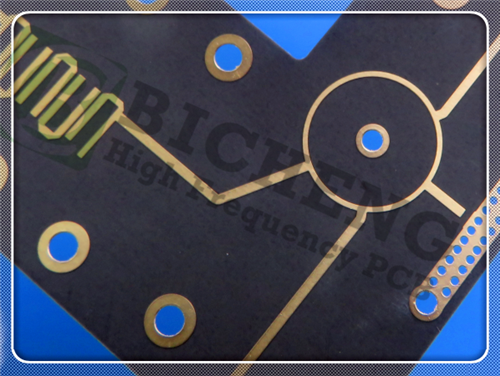
RTduroid 5880 PCB 2-layer 10mil Copper Filled Via for Exacting Stripline and Microstrip Circuit Applications |
|
|
|
|
|
|
|
1. Introduction of RT/duroid 5880
Rogers RT/duroid 5880 high - frequency laminates are crafted as PTFE composites strengthened by glass microfibers. Engineered specifically for the most demanding stripline and microstrip circuit applications, these laminates offer a distinct advantage. Thanks to the randomly arranged microfibers, they achieve an outstanding level of dielectric constant uniformity.
|
|
|
|
Not only is the dielectric constant of RT/duroid 5880 laminates consistent from one panel to another, but it also remains stable across a broad frequency spectrum. Moreover, its impressively low dissipation factor expands the applicability of RT/duroid 5880 laminates well into the Ku - band and even higher frequency ranges. This makes it an ideal choice for high - performance, frequency - sensitive electronic projects. |
|
|
|
2. Features
- Dielectric constant of 2.2 with tight tolerance 0.02 at 10 GHz/23°C
- Dissipation factor of 0.0009 at 10GHz
- Temperature coefficient of dielectric constant (TCDk) of -125 ppm/°C
- Low Moisture Absorption 0.02%
- CTE in X-axis of 31 ppm/°C, Y-axis of 48 ppm/°C and Z-axix of 237 ppm/°C
- Isotropic
|
|
|
|
3. Benefits
-Consistent electrical performance across a broad frequency spectrum
-Simple to cut, share, and machine into desired shapes
-Highly resistant to solvents and chemicals used in etching or plating edges and holes
-Perfectly suited for high-humidity or moisture-rich environments
-A proven and widely used material
-Offers the lowest electrical loss among reinforced PTFE materials |
|
|
|
4. PCB Stackup: 2-layer rigid PCB
Copper_layer_1 - 35 μm
RT/duroid 5880 - 0.254 mm (10mil)
Copper_layer_2 - 35 μm
|
|
|
|
| 5. PCB Construction Details: |
| |
| - Board dimensions: 50mm x 45 mm=1PCS, +/- 0.15mm
- Minimum Trace/Space: 5/4 mils
- Minimum Hole Size: 0.2mm
- No Blind vias.
- Finished board thickness: 0.4mm
- Finished Cu weight: 1oz (1.4 mils) outer layers
- Via plating thickness: 20 μm
- Surface finish: Immersion gold
- Top Silkscreen: White
- Bottom Silkscreen: No
- Top Solder Mask: Matt green
- Bottom Solder Mask: No
- Copper filling vias on designated IC Pad.
- 100% Electrical test used prior to shipment |
| |
| |
|
 |
|
|
|
|
6. PCB Statistics:
Components: 23
Total Pads: 40
Thru Hole Pads: 21
Top SMT Pads: 19
Bottom SMT Pads: 0
Vias: 42
Nets: 2 |
|
|
|
7. Type of artwork supplied: Gerber RS-274-X |
|
|
|
8. Quality standard: IPC-Class-2 |
|
|
|
9. Availability: worldwide |
|
|
|
10. Some Typical Applications:
- Microstrip and Stripline Circuits
- Millimeter Wave Applications
- Radar Systems
- Guidance Systems
- Point to Point Digital Radio Antennas |
|
|
|
|
|
|
|
|
|
|
|
|
|
NEXT: 2 - Layer, 20mil TLY - 5 PCB: Stable and Low - Loss Solution for Automotive Radar and Millimeter - Wave Applications |
|
|
|
|
|
|