|
|
|
Focus! 2-layer 40mil 1.016mm F4BTMS233 PCB Has an Unrivaled Low-Loss Feature |
|
|
|
|
|
|
|
1. F4BTMS Introduction
The F4BTMS series is the upgraded version of the F4BTM series, which has achieved a technological breakthrough in terms of material formulation and manufacturing processes. A significant amount of ceramics has been added to the material, and it is reinforced by ultra-thin and ultra-fine glass fiber cloth. Consequently, there are substantial improvements in its material performance and an expanded range of dielectric constants. It is a material of high reliability, making it suitable for aerospace applications and capable of substituting similar foreign products.
|
|
|
|
When a small amount of ultra-thin and ultra-fine glass fiber cloth and a large amount of specially formulated nano-ceramics, which are uniformly distributed and mixed with polytetrafluoroethylene resin, are incorporated, the adverse effects of glass fiber on electromagnetic wave propagation are significantly reduced. This results in decreased dielectric loss, enhanced dimensional stability, and reduced X/Y/Z anisotropy of the material. Additionally, it widens the usable frequency range, strengthens electrical strength, and improves thermal conductivity. The material also shows excellent low thermal expansion coefficient and stable dielectric temperature characteristics. |
|
|
|
The F4BTMS series features RTF low roughness copper foil as a standard, which reduces conductor loss and offers excellent peel strength. It can be utilized with either copper or aluminum bases. |
|
|
|
2. Features of F4BTMS233:
- Dielectric constant (Dk) of 2.33 at 10GHz
- Dissipation factor of 0.0010 at 10GHz, 0.0011 at 20GHz
- CTE x-axis of 35 ppm/°C, CTE y-axis of 40 ppm/°C, CTE z-axis of 220 ppm/°C, -55°C to 288°C
- Low thermal coefficient of Dk at-122 ppm/°C, -55°C to 150°C
- UL-94 V0
- Low Moisture absorption of 0.02%
|
|
|
|
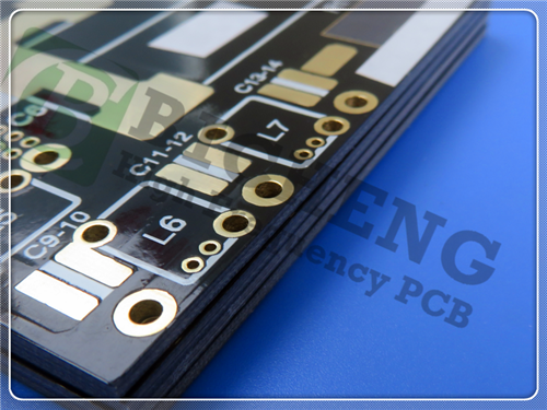
3. PCB Stackup: 2-layer rigid PCB
Copper_layer_1 - 35 μm
F4BTMS233 Core - 1.016 mm (40mil)
Copper_layer_2 - 35 μm |
|
|
|
| 4. PCB Construction Details: |
| |
| - Board dimensions: 40mm x 108 mm=1PCS, +/- 0.15mm
- Minimum Trace/Space: 5/4 mils
- Minimum Hole Size: 0.3mm - No Blind vias.
- Finished board thickness: 1.1mm
- Finished Cu weight: 1oz (1.4 mils) outer layers
- Via plating thickness: 20 μm
- Surface finish: OSP
- Top Silkscreen: White
- Bottom Silkscreen: No
- Top Solder Mask: Blue
- Bottom Solder Mask: No
- 100% Electrical test used prior to shipment |
| |
|
 |
|
|
|
|
5. PCB Statistics:
Components: 27
Total Pads: 62
Thru Hole Pads: 36
Top SMT Pads: 26
Bottom SMT Pads: 0
Vias: 41
Nets: 2
|
|
|
|
6. Type of artwork supplied: Gerber RS-274-X |
|
|
|
7. Quality standard: IPC-Class-2 |
|
|
|
8. Availability: worldwide |
|
|
|
9. Some Typical Applications:
- Aerospace equipment, space and cabin equipment
- Microwave, RF
- Radar, military radar
- Feed networks
- Phase-sensitive antennas, phased array antennas
- Satellite communications, and more. |
|
|
|
|
|
|
|
|
|
|
|
|
|
NEXT: F4BTMS1000 Double Layer 6.35mm Thick PCB with Advanced Technological Breakthroughs for Aerospace |
|
|
|
|
|
|