|
|
|
F4BTMS1000 Double Layer 6.35mm Thick PCB with Advanced Technological Breakthroughs for Aerospace |
|
|
|
|
|
|
|
1. F4BTMS Introduction
The F4BTMS series is an enhanced version of the F4BTM series, having made a significant technological leap in both material formulation and manufacturing processes. It incorporates a substantial amount of ceramics and is strengthened by ultra-thin and ultra-fine glass fiber cloth, thereby achieving remarkable enhancements in material performance. This includes a wider range of dielectric constants, making it a highly reliable material that is ideal for aerospace applications and capable of substituting similar foreign products.
|
|
|
|
incorporating a small amount of ultra-thin and ultra-fine glass fiber cloth along with a large quantity of uniformly distributed special nano-ceramics blended with polytetrafluoroethylene resin, the F4BTMS series minimizes the negative impact of glass fiber on electromagnetic wave propagation. This leads to several benefits, such as a reduction in dielectric loss, enhanced dimensional stability, and decreased X/Y/Z anisotropy of the material. Moreover, it broadens the usable frequency range, boosts electrical strength, and enhances thermal conductivity. Additionally, the material shows excellent characteristics of a low thermal expansion coefficient and stable dielectric temperature. |
|
|
|
As a standard feature, the F4BTMS series comes equipped with RTF low roughness copper foil. This not only reduces conductor loss but also provides excellent peel strength. It is versatile and can be used in conjunction with either copper or aluminum bases, offering flexibility in various applications. |
|
|
|
2. Features ㄗF4BTMS1000)
- Dielectric constant (Dk) of 10.2 at 10GHz
- Dissipation factor of .0020 at 10GHz, 0.0023 at 20GHz
- CTE x-axis of 16 ppm/°C, CTE y-axis of 18 ppm/°C, CTE z-axis of 32 ppm/°C, -55°C to 288°C
- Low thermal coefficient of Dk at-320 ppm/°C, -55°C to 150°C
- High Thermal conductivity of 0.81 W/mk
- Low Moisture absorption of 0.03%
|
|
|
|
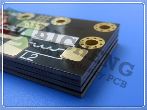
3. PCB Stackup: 2-layer rigid PCB
Copper_layer_1 - 35 μm
F4BTMS1000 Core - 6.35 mm (250mil)
Copper_layer_2 - 35 μm |
|
|
|
| 4. PCB Construction Details: |
| |
| - Board dimensions: 98mm x 98 mm=1PCS, +/- 0.15mm
- Minimum Trace/Space: 6/6 mils
- Minimum Hole Size: 0.6mm
- No Blind vias.
- Finished board thickness: 6.4mm
- Finished Cu weight: 1oz (1.4 mils) outer layers
- Via plating thickness: 20 μm
- Surface finish: Bare copper
- Top Silkscreen: No - Bottom Silkscreen: No
- Top Solder Mask: No
- Bottom Solder Mask: No
- 100% Electrical test used prior to shipment |
| |
|
 |
|
|
|
|
5. PCB Statistics:
Components: 20
Total Pads: 35
Thru Hole Pads: 21
Top SMT Pads: 14
Bottom SMT Pads: 0
Vias: 37
Nets: 2
|
|
|
|
6. Type of artwork supplied: Gerber RS-274-X |
|
|
|
7. Quality standard: IPC-Class-2 |
|
|
|
8. Availability: worldwide |
|
|
|
9. Some Typical Applications:
- Aerospace equipment, including space and cabin systems.
- Microwave and RF technologies.
- Military and commercial radar systems.
- Feed networks for various applications.
- Phase-sensitive and phased array antennas.
- Satellite communications, and numerous other applications. |
|
|
|
|
|
|
|
|
|
|
|
|
|
NEXT: 8-Layer 1.5mm RO4003CS10002M HDI Hybrid PCB: High-Frequency Game - Changer, Dual Performance & Cost Advantages |
|
|
|
|
|
|