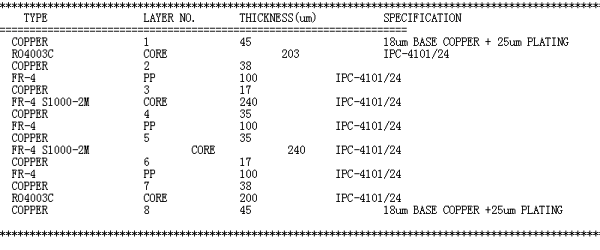
4. Basic PCB Specifications
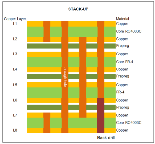
Board type: 8 layers
Material type: RO4003C + FR-4 Tg170 'C
Solder mask: Both sides, Green
Silkscreen print: Top side, white
Surface finish: ENIG
Total board thickness: 1.5mm +/- 10%
Board size: 87.5mm x 40.6mm=1 PCS
Minimum hole size: 0.2mm
Solder mask thickness: 10um
Minimum dielectric thickness: 100um
Minimum trace line width: 115um
Minimum spacing: 135um
Blind via: yes, L1-L2, L7-L8
Buried via: yes, L2-L7
Back drilled via: yes, L1-L6
Impedance controlled:
50 ohm, differential pairs, Top layer, 4mil / 4 mil trace/gap, reference layer 2
100 ohm, differential paris, top layer, 5mil / 6 mil trace/gap, reference layer 2
50 ohm, single end, top layer, 6 mil trace, reference layer 2
All 0.3mm vias are filled and capped in accordance with IPC 4761 Type VII. Edge plating is mandatory. |