|
|
|
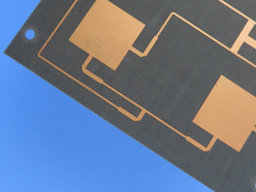
F4BTMS1000 2-Layer 0.508mm PCB Wangling Ultra High Thermal Conductivity Microwave Substrate for Phase Array Antennas |
|
|
|
|
|
|
|
1. F4BTMS Introduction
The F4BTMS series represents a significant technological evolution from its F4BTM predecessor, featuring an optimized material system combining nano-ceramic additives with precision-engineered glass fiber reinforcement in a PTFE matrix. This innovative formulation delivers superior dielectric stability across an extended Dk range while minimizing wave propagation interference - achieving reduced loss, enhanced dimensional control, and improved thermal/mechanical isotropy for demanding RF applications.
Engineered for mission-critical aerospace systems, these advanced laminates incorporate standard RTF copper foil for optimal conductor performance and compatibility with both copper/aluminum baseplates. The material's unique thermal characteristics - including exceptional CTE properties and temperature-stable dielectric behavior - position it as a competitive alternative to imported high-frequency solutions.
|
|
2. Features £¨F4BTMS1000) |
|
- Dielectric constant (Dk) of 10.2 at 10GHz
- Dissipation factor of .0020 at 10GHz, 0.0023 at 20GHz
- CTE x-axis of 16 ppm/°C, CTE y-axis of 18 ppm/°C, CTE z-axis of 32 ppm/°C, -55°C to 288°C
- Low thermal coefficient of Dk at-320 ppm/°C, -55°C to 150°C - High Thermal conductivity of 0.81 W/mk
- Low Moisture absorption of 0.03% |
|
|
|
3. PCB Stack-up: 2-layer Rigid PCB
Copper_layer_1 - 35 μm
F4BTMS1000 Core - 0.508 mm (20mil)
Copper_layer_2 - 35 μm
|
|
|
|
| 4. PCB Construction details: |
| |
| - Base material: F4BTMS1000
- Layer count: 2 layers
- Board dimensions: 85mm x 40 mm=1PCS, +/- 0.15mm
- Minimum Trace/Space: 4/4 mils
- Minimum Hole Size: 0.3mm
- No Blind vias.
- Finished board thickness: 0.6mm
- Finished Cu weight: 1oz (1.4 mils) outer layers
- Via plating thickness: 20 μm
- Surface finish: OSP
- Top Silkscreen: No
- Bottom Silkscreen: No
- Top Solder Mask: No
- Bottom Solder Mask: No
- 100% Electrical test used prior to shipment |
| |
|
 |
| |
|
|
|
5. PCB Statistics:
Components: 21
Total Pads: 60
Thru Hole Pads: 33
Top SMT Pads: 27
Bottom SMT Pads: 0
Vias: 41
Nets: 2
|
|
|
|
6. Type of artwork supplied: Gerber RS-274-X |
|
|
|
7. Quality standard: IPC-Class-2 |
|
|
|
8. Availability: worldwide |
|
|
|
9. Some Typical Applications:
- Aerospace equipment, space and cabin equipment
- Microwave, RF
- Radar, military radar
- Feed networks
- Phase-sensitive antennas, phased array antennas
- Satellite communications, and more. |
|
|
|
|
|
|
|
|
|
|
|
|
|
NEXT: 10-layer IT-180ATC FR-4 HDI PCB 1.6mm Circuit Boards with Green Solder Mask and Immersion Gold for Lead Free Assembly |
|
|
|
|
|
|