|
|
|
F4BM220 PCB 2-Layer 1.575mm Precision PTFE Material for Low Loss and PIM Critical Applications From Wangling |
|
|
|
|
|
|
|
1. Introduction of F4BM220
Wangling's F4BM220 laminates represent a scientifically engineered PTFE composite solution, combining fiberglass cloth with polytetrafluoroethylene resin and film to deliver superior electrical performance over conventional F4B220 materials. These high-performance laminates feature reduced dielectric loss, enhanced insulation resistance, and improved stability - providing a cost-competitive alternative to imported equivalents.
The series offers two optimized copper foil configurations: F4BM220 with ED copper for standard applications, and F4BME220 featuring reverse-treated foil (RTF) for designs requiring exceptional PIM performance, precision line control, and minimized conductor loss. Through precise adjustment of the PTFE-to-fiberglass ratio, both variants maintain excellent dielectric constant control while delivering industry-leading dimensional stability and thermal performance - with fiberglass content strategically balanced to optimize the thermal expansion coefficient, temperature drift, and loss characteristics.
|
|
2. Features £¨F4BM220) |
|
- Dielectric constant (Dk) of 2.2±0.04 at 10GHz
- Dissipation factor of .001 at 10GHz
- CTE x-axis of 25 ppm/°C, CTE y-axis of 34 ppm/°C, CTE z-axis of 240 ppm/°C, -55°C to 288°C
- Thermal coefficient of Dk at-142 ppm/°C, -55°C to 150°C
- Moisture absorption of ≤0.08%
- Flammability of UL-94 V0 |
|
|
|
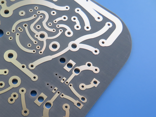
3. PCB Stack-up: 2-layer Rigid PCB
Copper_layer_1 - 35 μm
F4BM220 Core - 1.575 mm
Copper_layer_2 - 35 μm
|
|
|
|
| 4. PCB Construction details: |
| |
| - Base material: F4BM220
- Layer count: 2 layers
- Board dimensions: 130.5mm x 103 mm=1PCS, +/- 0.15mm
- Minimum Trace/Space: 4/6 mils
- Minimum Hole Size: 0.3mm
- No Blind vias.
- Finished board thickness: 1.7mm
- Finished Cu weight: 1oz (1.4 mils) outer layers
- Via plating thickness: 20 μm
- Surface finish: Electroless Nickle Immersion Gold (ENIG)
- Top Silkscreen: No
- Bottom Silkscreen: No
- Top Solder Mask: No
- Bottom Solder Mask: No
- 100% Electrical test used prior to shipment |
| |
|
 |
| |
|
|
|
5. PCB Statistics:
Components: 43
Total Pads: 94
Thru Hole Pads: 56
Top SMT Pads: 38
Bottom SMT Pads: 0
Vias: 51
Nets: 2
|
|
|
|
6. Type of artwork supplied: Gerber RS-274-X |
|
|
|
7. Quality standard: IPC-Class-2 |
|
|
|
8. Availability: worldwide |
|
|
|
9. Some Typical Applications:
- Microwave, RF, and radar systems
- Phase shifters
- Power dividers, couplers, combiners
- Feed networks
- Phase-sensitive antennas, phased array antennas
- Satellite communications
- Base station antennas |
|
|
|
|
|
|
|
|
|
|
|
|
|
NEXT: F4BTMS430 2-Layer PCB Wangling 3.175mm Aerospace Grade Ceramic PTFE Composite with Enhanced Dk Range and Stability |
|
|
|
|
|
|