|
|
|
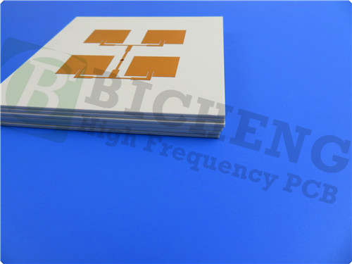
Customized Double Sided 0.127 mm 5mil TFA294 Material PCB ENEPIG Surface Finish |
|
|
|
|
|
|
|
1. Introduction of TFA series
The dielectric layer of the TFA series Polytetrafluoroethylene ceramic composite dielectric substrate is composed of PTFE resin and ceramics, produced through a novel process rather than the traditional method of impregnating glass fiber cloth with resin to create prefabricated sheets. Instead, this series employs a unique lamination technique to press these sheets, resulting in a material that boasts exceptional electrical, thermal, and mechanical properties. It achieves an excellent dielectric constant comparable to aerospace-grade materials, making it a high-frequency and high-reliability option that can effectively replace similar foreign products.
|
|
|
|
Notably, this series does not contain glass fiber cloth. Instead, it incorporates a substantial amount of uniform special nano-ceramics mixed with resin, which eliminates the fiberglass effect during electromagnetic wave propagation. This results in outstanding frequency stability and minimal dielectric loss. The material also minimizes X/Y/Z anisotropy and features a low thermal expansion coefficient comparable to that of copper foil, along with stable dielectric temperature characteristics. |
|
|
|
The dielectric constant for this series offers four options: 2.94, 3.0, 6.15, and 10.2, corresponding to part numbers TFA294, TFA300, TFA615, and TFA1020, respectively. |
|
|
|
2. Features of TFA294:
- Dielectric constant (Dk) of 2.94 at 10GHz
- Dissipation factor of .0010 at 10GHz and 20 GHz, 0.0012 at 40 GHz
- Low TCDK at -5 ppm/°C, -55°C to 150°C
- CTE x-axis of 18 ppm/°C, CTE y-axis of 18 ppm/°C, CTE z-axis of 32 ppm/°C, -55°C to 288°C
- Thermal conductivity of 0.59 W/mk
- Moisture absorption of 0.03%
- UL 94-V0
|
|
|
|
3. PCB Stackup: 2-layer rigid PCB
Copper_layer_1 - 35 μm
TFA294 Core - 0.127 mm (5mil)
Copper_layer_2 - 35 μm |
|
|
|
| 4. PCB Construction Details: |
| |
| - Board dimensions: 58.1mm x 66 mm=1PCS, +/- 0.15mm
- Minimum Trace/Space: 4/5 mils
- Minimum Hole Size: 0.2mm
- No Blind vias.
- Finished board thickness: 0.25mm
- Finished Cu weight: 1oz (1.4 mils) outer layers
- Via plating thickness: 20 μm
- Surface finish: ENEPIG
- Top Silkscreen: No
- Bottom Silkscreen: No
- Top Solder Mask: No
- Bottom Solder Mask: No
- 100% Electrical test used prior to shipment |
| |
|
 |
|
|
|
|
5. PCB Statistics:
Components: 10
Total Pads: 26
Thru Hole Pads: 15
Top SMT Pads: 11
Bottom SMT Pads: 0
Vias: 9
Nets: 2
|
|
|
|
6. Type of artwork supplied: Gerber RS-274-X |
|
|
|
7. Quality standard: IPC-Class-2 |
|
|
|
8. Availability: worldwide |
|
|
|
9. Some Typical Applications:
- Aerospace equipment, space, in-cabin equipment, aircraft;
- Microwaves, antennas, phase-sensitive antennas;
- Early warning radars, airborne radars, etc.;
- Phased array antennas, beamforming networks;
- Satellite communications, navigation;
- Power amplifiers. |
|
|
|
|
|
|
|
|
|
|
|
|
|
NEXT:TLX Serie 2-layer Low DK2.55 Taconic TLX-8 High Frequency PCB 30mil Immersion Gold |
|
|
|
|
|
|