Shenzhen Bicheng Electronics Technology Co., Ltd
深圳市碧澄电子科技有限公司
+86-755-27374946
info@bicheng-enterprise.com
WELCOME TO BICHENG


0.8mm 2-layer Ceramics and PPO Composites High Frequency PCB Wangling TP440 for Beidou

Shipped: 25th-NOV-2024  

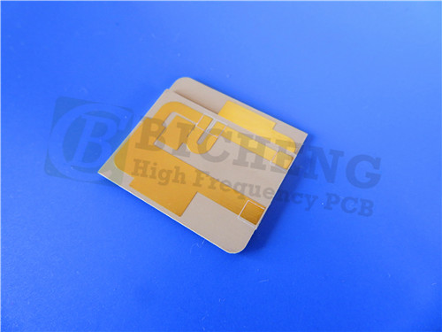
1. Introduction of Wangling TP
TP material is a unique high-frequency thermoplastic material in the industry. The dielectric layer of TP-type laminates consists of ceramics and polyphenylene Oxide resin (PPO), without fiberglass reinforcement. The dielectric constant can be precisely adjusted by adjusting the ratio between ceramics and PPO resin. The production process is special, and it has excellent dielectric performance and high reliability. TP refers to the smooth surface material without copper cladding, TP-1 refers to the material with copper cladding on one side, and TP-2 refers to the material with copper cladding on both sides.


2. Features
1.The dielectric constant can be arbitrarily selected within the range of 3 to 25 according to circuit requirements, and it is stable. Common dielectric constants include 3.0, 4.4, 6.0, 6.15, 9.2, 9.6, 10.2, 11, 16, and 20. The dielectric loss is low, and the loss increases as the frequency increases, but the change is not significant within 10 GHz.
2.Long-term operating temperature ranges from -100°C to +150°C. It has excellent low-temperature resistance. When the temperature exceeds 180°C, the material may deform, the copper foil may peel off, and there may be significant changes in electrical performance.
3.The thinnest thickness is 0.5mm, and it is available in various thicknesses and can be customized.
4.It is resistant to radiation and has low outgassing.
5.Ideal material for Beidou, missile-borne, fuze, and miniaturized antennas.
6.The adhesion between copper foil and dielectric is more reliable than ceramic substrates with vacuum coating. The material is easy to machine and can be processed through drilling, turning, grinding, shearing, etching, and other methods, which ceramic substrates cannot achieve.

 
3. Typical Model Number List
TP300 (DK3.0)
TP440 (DK4.4)
TP600 (DK6.0)
TP615 (DK6.15)
TP960 (DK9.6)
TP1020 (DK10.2)
TP1050 (DK10.5)
TP1100 (DK11)
TP1600 (DK16)
TP2000 (DK20)
TP2200 (DK22)
TP2500 (DK25)
 
4. PCB Stackup(TP440): 2-layer rigid PCB
Copper_layer_1 - 35 μm
TP440 Core - 0.8 mm
Copper_layer_2 - 35 μm


5. PCB Construction details:
 
- Board dimensions: 33.12mm x 42.5 mm=1PCS, +/- 0.15mm
- Minimum Trace/Space: 6/9 mils
- Minimum Hole Size: 0.3mm
- No Blind vias.
- Finished board thickness: 0.9mm
- Finished Cu weight: 1oz (1.4 mils) outer layers
- Via plating thickness: 20 μm
- Surface finish: Immersion Gold
- Top Silkscreen: No
- Bottom Silkscreen: No
- Top Solder Mask: No
- Bottom Solder Mask: No
- 100% Electrical test used prior to shipment


6. PCB Statistics:
Components: 5
Total Pads: 15
Thru Hole Pads: 9
Top SMT Pads: 6
Bottom SMT Pads: 0
Vias: 8
Nets: 1
 
7. Type of artwork supplied: Gerber RS-274-X
 
8. Quality standard: IPC-Class-2
 
9. Availability: worldwide
10. Some Typical Applications:
- GPS antenna
- missile-borne
- fuze
- miniaturized antennas


NEXT:2-layer 20 mil Thickness Taconic DF 0.0011 TSM-DS3 for High-power Applications


About Us
Products
Solutions
Contact Us


Antenna, Mobile Internet
Address:
6-11C Shidai Jingyuan, Fuyong, Baoan, Shenzhen, Guangdong, China 518103


Wireless Infrastructure
Phone:
86-755-27374946


Millimeter Wave Radar
Email:
info@bicheng-enterprise.com


Aerospace
 
WeChat:
bichengpcb


Satellite Navigation
 
Skype:
vickyxie0315@outlook.com


Power Amplifier


IoT


in fb yt quora


Copyright  © Shenzhen Bicheng Electronics Technology Co., Ltd. All rights reserved