|
|
|
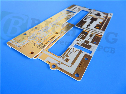
2-layer 20 mil Thickness Taconic DF 0.0011 TSM-DS3 for High-power Applications |
|
|
|
|
|
|
|
1. Introduction of TSM-DS3 TSM-DS3 is a ceramic-filled reinforced material with very lowfiberglass content (~ 5%) that rivals epoxies in fabricating large format complex multilayers. TSM-DS3 is a thermally stable, industry leading low loss core (Df = 0.0011 at 10 GHz) that can be manufactured with thepredictability and consistency of the best fiberglass reinforced epoxies. TSM-DS3 was developed for high power applications (TC = 0.65 W/m*K) where it is necessary for the dielectric material to conductheat away from other heat sources in a PWB design. TSM-DS3 was also developed to have very low coefficients of thermal expansionfor demanding thermal cycling. |
|
|
|
2. Features (TSM-DS3)
- Dielectric constant of 3.0 with tight tolerance 0.05 at 10 GHz/23°C
- Dissipation factor of 0.0014 at 10GHz
- High Thermal conductivity (unclad) of 0.65 W/MK
- Low Moisture Absorption 0.07%
- Matched to copper CTE in X-axis of 10 ppm/°C, Y-axis of 16 ppm/°C and Z-axix of 23 ppm/°C |
|
|
|
3. Benifits
- Low (~5%) Fiberglass Content
- Dimensional Stability Rivals Epoxy
- Enables Large Format High Layer Count PCBs
- Builds Complex PCBs in Yield w/ Consistency and Predictability
- Temperature Stable Dk ± 0.25% (-30 to 120°C)
- Compatible With Resistive Foils |
|
|
|
4. PCB Stackup: 2-layer rigid PCB
Copper_layer_1 - 35 μm
TSM-DS3 - 0.508 mm (20 mil)
Copper_layer_2 - 35 μm |
|
|
|
|
|
|
| 5. PCB Construction details: |
- Board dimensions: 92.3mm x 41.52 mm=2Types = 2PCS, +/- 0.15mm
- Minimum Trace/Space: 5/9 mils
- Minimum Hole Size: 0.5mm
- No Blind vias.
- Finished board thickness: 0.5mm
- Finished Cu weight: 1oz (1.4 mils) outer layers
- Via plating thickness: 20 μm
- Surface finish: Immersion Silver
- Top Silkscreen: White
- Bottom Silkscreen: No
- Top Solder Mask: Green
- Bottom Solder Mask: No
- 100% Electrical test used prior to shipment
|
| |
| |
| |
| |
| |
| |
|
 |
|
|
6. PCB Statistics:
Components: 12
Total Pads: 28
Thru Hole Pads: 17
Top SMT Pads: 11
Bottom SMT Pads: 0
Vias: 25
Nets: 2 |
|
|
|
7. Type of artwork supplied: Gerber RS-274-X |
|
|
|
8. Accepted standard: IPC-Class-2 |
|
|
|
9. Availability: worldwide |
|
|
|
10. Some Typical Applications:
- Couplers
- Phased Array Antennas
- Radar Manifolds
- mmWave Antenna/Automotive
- Oil Drilling
- Semiconductor/ATE Testing
|
|
|
|
|
|
|
|
|
|
|
|
|
|
NEXT:F4BM220 High Frequency PCB: A 2-Layer Design with 1.0mm Thickness and Immersion Gold |
|
|
|
|
|
|