|
|
|
|
Why Do PCB Boards Use Resin Plugging and capped?
|
|
|
Overview of Resin Plugging
|
|
|
Resin plugging involves using conductive or non-conductive resin to fill various types of holes, such as mechanical through-holes and blind buried holes, through printing and all possible methods. The purpose is to effectively plug the holes. |
|
|
|
|
|
|
|
|
|
|
|
Purpose of Resin Plugging |
|
|
1. After filling various blind buried holes with resin, it facilitates a decrease in vacuum during lamination. |
|
|
2.
After filling various blind buried holes with resin, it facilitates a decrease in vacuum during lamination. |
|
|
3. It effectively utilizes three-dimensional space, enabling interconnection between layers through hole stacking technology. |
|
|
4. By designing surface mount components over the holes, it allows for higher density routing. |
|
|
5. It can eliminate impurities from entering conductive holes or prevent the inclusion of corrosive contaminants. |
|
|
|
|
|
Advantages and Disadvantages of Resin Plugging and Its Applications |
|
|
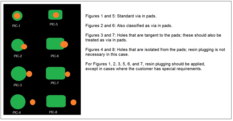
When design requirements necessitate plugging through-holes, or when through-holes are not allowed to appear red, and there are via in pads, it is recommended to use resin plugging. It is also advised when through-holes are located at BGA solder points. |
|
|
|
|
|
Advantages of Plugging |
|
|
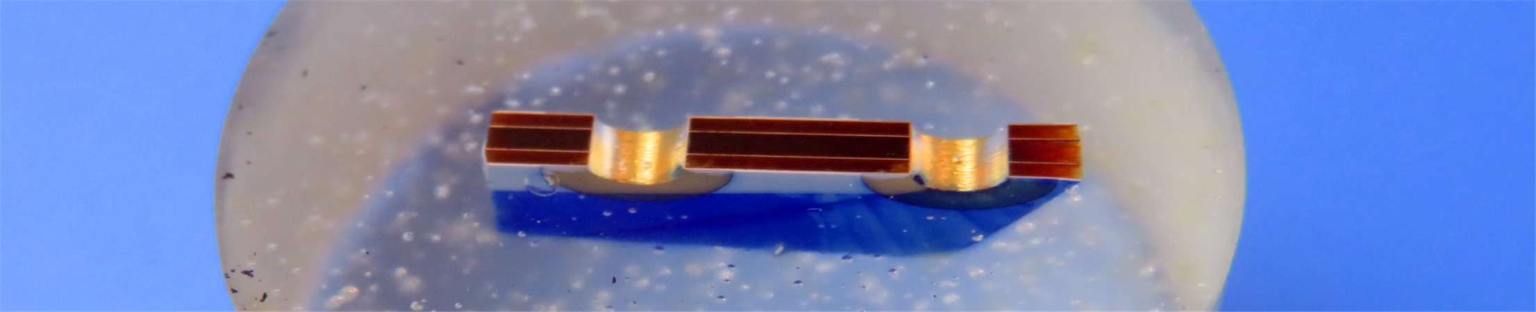
Through-holes are often present in pads for heat dissipation. To prevent solder from flowing to the layer below the pad, applying resin plugging to through-holes can lead to fuller plugs and enhance the product's lifespan. |
|
|
|
|
|
Disadvantages of Plugging |
|
|
Due to higher production costs, a more complex process, and the expensive equipment required, the unit price of resin plugging is generally higher. |
|
|
|
|
|
Through-holes above a BGA are typically defined as via in pads, which need resin plugging. The resin on top is then plated and capped for easier product soldering. Aside from BGAs, if a product requires resin plugging for all through-holes, the through-holes above the surface mount components are also defined as via in pads. |
|
|
|
|
|
|
|
|
|
|
|
Resin Plugging Process: |
|
|
1.
Material Preparation (for multilayer boards, the process occurs after lamination) |
|
|
2.
Resin Drilling |
|
|
3. Copper Plating |
|
|
4. Board Plating |
|
|
5. Resin Plugging |
|
|
6. Resin Grinding |
|
|
7. Copper Reduction |
|
|
(Performed according to the finished copper thickness and requirements for line width and spacing) |
|
|
8. QC Inspection |
|
|
|
|
|
Production and Manufacturing of Resin Plugging |
|
|
The manufacturing capabilities for resin plugging include: |
|
|
|
|
|
Hole Diameter: Generally ranges from 0.1 mm to 0.8 mm. |
|
|
Board Thickness: Ranges from 0.4 mm to 8.0 mm. |
|
|
Types of Plugging: Includes buried via plugging, blind via?plugging, and through-hole plugging. |
|
|
Resin Types: Further categorized into insulating resin plugging and conductive resin plugging. At Bicheng, we use copper paste instead of conductive resin. |
|
|
|
|
|
1. Drilling Production |
|
|
For holes that require via in pads, after optimizing the drilling, move the via in pad to another layer, naming them DRL-VIP, with the attribute set as the board's drilling attribute. |
|
|
|
|
|
For resin plugging holes, create a drill file that is 0.15 mm larger than the diameter of the plugging hole, naming it DRL-RP. |
|
|
|
|
|
When the via in pad is a blind via requiring resin plugging, simply copy the blind via to another layer and enlarge it by 0.15 mm, naming it DRL-RP. If there are multiple blind vias, the naming for the drill files can be DRL1-2RP, DRL3-4RP, etc. |
|
|
|
|
|
It is essential to note that if the via in pads are blind vias and there are also through-holes, all via in pads must be selected for resin plugging. Remember not to overlook the vias on the BGA, as they should not have resin plugging applied. |
|
|
|
|
|
2. Circuit Production |
|
|
For the layer circuits of resin plugging holes, a compensation of 1.5-2 mils is required, and it is advisable to add as much as possible. |
|
|
|
|
|
3. Solder Mask Production |
|
|
For the through-holes of resin plugging, do not apply solder mask plugging. The solder mask openings corresponding to the resin plugging holes should follow the original file (if there are irregular openings for all holes on the board, it is necessary to confirm in advance whether to delete them). |
|
|
|
|
|
|
|