|

|
|
|
|
|
What Circuit Boards Do We Do? (57)
|
|
|
F4BTM High Frequency PCB
|
|
|
|
|
|
Introduction |
|
|
Wangling*s F4BTM series laminates are fiberglass cloth, nano-ceramic fillers, and PTFE resin, followed by strict pressing processes. They are based on the F4BM dielectric layer, with the addition of high dielectric and low loss nano-level ceramics, resulting in higher dielectric constant, improved heat resistance, lower thermal expansion coefficient, higher insulation resistance, and better thermal conductivity, while maintaining low loss characteristics |
|
|
|
|
|
F4BTM and F4BTME share the same dielectric layer but use different copper foils: F4BTM is paired with ED copper foil, while F4BTME is paired with reverse-treated (RTF) copper foil, offering excellent PIM performance, more precise line control, and lower conductor loss. |
|
|
|
|
|
Features |
|
|
F4BTM offers a wide range of features. With a DK range from 2.98 to 3.5, it provides flexibility in design. The addition of ceramics further enhances its performance, making it suitable for demanding applications. This material is available in various thicknesses and sizes, catering to different project requirements while offering cost savings. Its commercialization and suitability for large-scale production make it a highly cost-effective choice. Additionally, F4BTM exhibits radiation-resistant and low out-gassing properties, ensuring its reliability even in challenging environments. |
|
|
|
|
|
|
|
|
|
|
|
PCB Capability |
|
|
Our PCB manufacturing capabilities cover a wide range of options. We can handle various layer counts, including single-sided, double-sided, multilayer, and hybrid PCBs. |
|
|
|
|
|
For copper weight, we offer options of 1oz (35µm), and 2oz (70µm), allowing flexibility in conductivity requirements. |
|
|
|
|
|
When it comes to dielectric thickness (or overall thickness), we provide a comprehensive selection of options ranging from 0.25mm to 12.0mm, catering to different design specifications. |
|
|
|
|
|
The maximum PCB size we can accommodate is 400mm X 500mm, ensuring sufficient space for your project. |
|
|
|
|
|
We offer a variety of solder mask colors, including green, black, blue, yellow, red, and more, allowing for customization and visual distinction. |
|
|
|
|
|
Regarding surface finish, we support several options such as bare copper, HASL, ENIG, immersion silver, immersion tin, OSP, pure gold, ENEPIG, and more, ensuring compatibility with your specific requirements. |
|
|
|
|
|
| |
PCB Capability (F4BTM) |
PCB Material: |
PTFE / glass fiber cloth / Nano-ceramic filler |
Designation (F4BTM ) |
F4BTM |
DK (10GHz) |
DF (10 GHz) |
F4BTM298 |
2.98±0.06 |
0.0018 |
F4BTM300 |
3.0±0.06 |
0.0018 |
F4BTM320 |
3.2±0.06 |
0.0020 |
F4BTM350 |
3.5±0.07 |
0.0025 |
Layer count: |
Single Sided, Double Sided PCB, Multilayer PCB, Hybrid PCB |
Copper weight: |
1oz (35µm), 2oz (70µm) |
Dielectric thickness (or overall thickness) |
0.25mm, 0.508mm, 0.762mm, 0.8mm, 1.0mm, 1.016mm, 1.27mm, 1.524mm, 2.0mm, 3.0mm, 4.0mm, 5.0mm, 6.0mm, 8.0mm, 10.0mm, 12.0mm |
PCB size: |
≒400mm X 500mm |
Solder mask: |
Green, Black, Blue, Yellow, Red etc. |
Surface finish: |
Bare copper, HASL, ENIG, Immersion silver, Immersion tin, OSP, Pure gold, ENEPIG etc.. |
|
|
|
|
|
|
|
Applications |
|
|
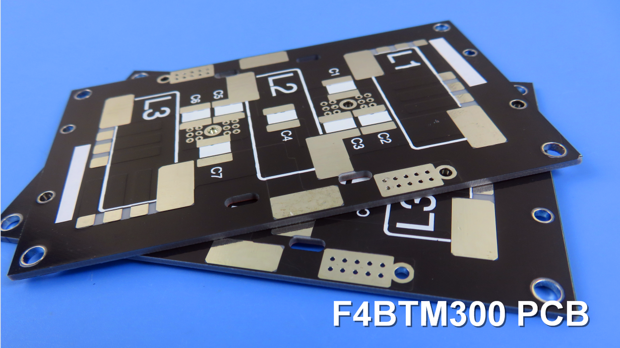
The screen displays a DK 3.0 F4BTM PCB, constructed on a 1.524mm substrate and featuring HASL surface finishes. |
|
|
|
|
|
F4BTM PCBs are utilized in various applications, including Antenna, Mobile Internet, Sensor Network, Radar, Millimeter Wave Radar, Aerospace, Satellite Navigation, and Power Amplifier etc. |
|
|
|
|
|
Thank you. I*ll see you next time. |
|
|
|
|
|
|
|
|
|
|
|
|
|
|
|
|
|
|