| |
 |
| |
|
|
|
|
|
| |
|
What is a Blind Via Hole in High Frequency PCB? |
|
|
|
| |
|
1. Brief Introduction to Blind Via Hole |
|
|
|
| |
|
In high-frequency PCB design, a blind via hole refers to a hole that only connects one side of the PCB, connecting from the outer layer to the inner layer, and does not penetrate the entire circuit board.
"The smoothness of signal transmission often depends on the clever layout of blind via hole." Thus, the importance of blind via hole in high-frequency signal transmission cannot be underestimated. They not only save space but also optimize circuit layout, helping to reduce the length of signal paths, thereby lowering signal loss and improving signal integrity. This is crucial for high-frequency applications, as signal attenuation and distortion can significantly affect performance at higher frequencies. |
|
|
| |
|
|
|
|
| |
|
2. Impact of Blind Via Layout |
|
|
| |
|
2.1 Signal Path Length
Blind vias reduce the distance of signal transmission, enhancing signal efficiency.
2.2 Impedance Control
Properly arranged blind vias help maintain consistent impedance, reducing reflections and distortion.
2.3 Crosstalk Suppression
Strategically placed vias minimize interference between adjacent signals, improving signal integrity.
2.4 Layer Transition
Blind vias effectively manage signal transitions between multiple layers, reducing parasitic capacitance and inductance.
2.5 Return Path
They provide an effective return path, helping to reduce electromagnetic interference (EMI). |
|
|
| |
|
|
|
|
| |
|
3. Considerations for Selecting Blind Via Hole |
|
|
| |
|
Consideration Factors |
Specifics |
Electrical Performance |
Smaller Blind Via Holes for high-frequency signals to reduce losses. Ensure impedance matching. |
Manufacturing Process |
Consider manufacturer's capacity. Different drilling techs have size and pitch requirements. |
Mechanical Strength |
Avoid thin hole walls. Select size based on load. |
Pitch Requirements |
Follow design rules for min pitch. Ensure EMC with proper spacing. |
Heat Dissipation |
Choose sizes and pitches for effective heat dissipation in high-power apps. |
Prototype Testing |
Verify design through testing and adjust if needed. |
|
|
|
| |
|
|
|
|
| |
|
4.The Advantange of Rogers RO4533 PCB |
|
|
| |
|
When mentioning blind via holes in the design and application of high-frequency PCBs, what impresses me the most is Rogers RO4533.
Rogers RO4533 Substrate is a ceramic-filled glass hydrocarbon-based reinforced laminate that boasts excellent mechanical and electrical properties and performs well within a wide frequency range. Its typical glass transition temperature surpasses 280°C (536°F), causing a minimal z-axis CTE and exceptional reliability for plated through-holes. When blind vias are fabricated, it can provide good support in terms of the base material's properties, ensuring the dimensional accuracy and surface quality of the blind vias. This is conducive to achieving high-precision blind via processing, thereby enhancing the performance and reliability of high-frequency circuits.
Moreover,RO4533 laminates are offered as halogen-free to comply with the strictest 'green' standards, and they come with RoHS-compliant flame-retardant technology for applications that require UL94 V-0 certification. |
|
|
| |
|
|
|
|
| |
|
4.1 Features and Benefits |
|
|
| |
|
- Low Loss (DF 0.0025) and Low Dk (3.3): Rogers RO4533 high-frequency PCB Presents a low Passive Intermodulation (PIM) response, making it appropriate for a broad spectrum of applications.
- Thermoset Resin System: Aligns with standard PCB fabrication procedures, ensuring ease of operation.
- Excellent Dimensional Stability: Delivers greater output on larger panel sizes, enhancing manufacturing productivity.
- Uniform Mechanical Properties: Preserves mechanical integrity during handling, reducing the likelihood of damage.
- High Thermal Conductivity(0.6 W/mK): Boosts power handling capacities, enabling enhanced performance in challenging applications.
|
|
|
| |
|
|
|
|
| |
|
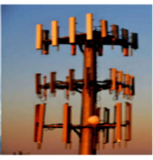
4.2 Major Applications |
|
|
| |
|
Cellular infrastructure base station antennas
WiMAX antenna networks |
|
|
| |
|
|
|
|
| |
|
|
|
|
| |
|
|
|
|
| |
|
5. Future Outlook |
|
|
| |
|
In the future, as technology continues to advance, blind via technology will play an even greater role in the field of high-frequency PCBs. Through scientifically rational blind via layouts, we can ensure the smooth transmission of high-frequency signals, laying a solid foundation for the high performance and reliability of electronic products. |
|
|
| |
|
|
|
|
| |
|
Founded in 2003, Shenzhen Bicheng Electronics Technology Co., Ltd is an established high frequency PCB supplier and exporter in Shenzhen, China, serving customers worldwide.
We are devoted to delivering high-frequency PCB products and solutions of the highest quality, along with customized service. Feel free to consult and contant at any time !
Visit https://www.bicheng-enterprise.com to learn more.
Unlock its full potential by contacting Vicky at v.xie@bichengpcb.com. |
|
|
| |
|
|
|
|
| |
|
|
|
|
| |
|
|
|
|
| |
|
|
|
| |
|
|
|
| |
|
|
|
|
|