| |
 |
| |
|
|
|
|
|
| |
|
What is Via Plating Thickness in High Frequency PCB ? |
|
|
|
| |
|
1. Reason for Copper Plating |
|
|
|
| |
|
"Via plating thickness" refers to the thickness of the copper plating on vias. The walls of vias need to be copper - plated. This is because copper is an excellent conductive material. Copper plating ensures that vias have good electrical conductivity, thus guaranteeing that signals and power can be smoothly transmitted between different layers. At the same time, the copper - plated layer can also protect the via walls from corrosion and other damages. |
|
|
| |
|
|
|
|
| |
|
2. Importance of Via Plating Thickness |
|
|
| |
|
The thickness of via copper plating significantly impacts PCB performance. Insufficient thickness can lead to excessive via resistance. In high-frequency circuits, this causes signal attenuation and distortion, affecting signal integrity. It may also reduce mechanical strength and corrosion resistance, potentially causing via damage during the PCB's service life.
Conversely, excessive thickness can make via size smaller, affecting connections and increasing production cost due to more copper-plating material. Thus, precise control of via copper plating thickness is crucial in PCB manufacturing. |
|
|
| |
|
|
|
|
| |
|
3. How to Select Via Plating Thickness |
|
|
| |
|
Application requirements lead the way. High - speed digital circuits need thicker plating for better signal integrity. For example, data center servers demand precise thickness. But for low - power, low - frequency consumer electronics like handheld calculators, thinner plating suffices and cuts costs. Manufacturing capabilities count too. Different factories have their own strengths. The chosen thickness must fit the factory's skills, or quality and performance problems may follow. Cost is also key. Thick plating means higher costs, while thin plating may save money but could lead to rework if it affects performance.
|
|
|
| |
|
|
|
|
| |
|
4. The Distinct Advantange of Taconic TLX-0 PCB |
|
|
| |
|
When it comes to the application of board tooling holes in high-frequency PCBs, I can't help but think of Taconic TLX series PCBs. Especially, as a PTFE-based glass fiber laminate, TLX-0 laminate has stable electrical performance and outstanding advantages regarding via plating thickness. |
|
|
| |
|
|
|
|
| |
|
4-1. The TLX series laminate |
|
|
| |
|
 |
|
|
| |
|
|
|
|
| |
|
4.1 Low & Stable Dielectric Constant |
|
|
| |
|
The dielectric constant of TLX-0 PCB is 2.45, staying fairly stable from 1 GHz to 10 GHz. Minimal fluctuation means less impact on signal speed and crosstalk, helping maintain signal integrity. |
|
|
| |
|
|
|
|
| |
|
4.2 Low Loss Tangent |
|
|
| |
|
At 10 GHz, its loss tangent is 0.0012. So, under varying via plating thicknesses, signal energy loss through vias is small, reducing attenuation, crucial for high - frequency transmission. Let's take a look at the comparison of Dk values and Df values between TLX-0 and other PCBs in the TLX series. |
|
|
| |
|
|
|
|
| |
|
Property |
Test Method |
TLX Typical Values |
TLX-7 |
TLX-8 |
TLX-9 |
TLX-0 |
Dk @ 10 GHz |
IPC-650 2.5.5.3 |
2.65 |
2.60 |
2.55 |
2.50 |
2.45 |
Df @ 1.9 GHz |
IPC-650 2.5.5.5.1 |
0.0016 |
0.0014 |
0.0012 |
0.0010 |
0.0009 |
Df @ 10 GHz |
IPC-650 2.5.5.5.1 |
0.0022 |
0.0020 |
0.0017 |
0.0015 |
0.0012 |
|
|
|
| |
|
|
|
|
| |
|
According to the table, when comparing the TLX series PCBs, we can see that TLX-0 has the lowest dielectric constant. This is beneficial for reducing signal transmission delay and signal distortion, especially in high-frequency circuits, as it can better maintain signal integrity and transmission speed. It also has the lowest dissipation factor that can reduce signal energy loss, improve circuit efficiency, and extend the battery life and service life of electronic devices. |
|
|
| |
|
|
|
|
| |
|
4.3 Good Dimensional Stability |
|
|
| |
|
With a low thermal expansion coefficient, TLX - 0 substrate has little size change. During via plating, regardless of copper thickness alteration, via size and shape stay consistent, ensuring connection accuracy and minimizing signal reflection and loss. |
|
|
| |
|
|
|
|
| |
|
4.4 Wide Dielectric Thickness Range |
|
|
| |
|
The dielectric thickness spans 0.127 mm to 6.35 mm. Designers can pick suitable ones to pair with via plating thickness for optimal electrical and signal performance. |
|
|
| |
|
|
|
|
| |
|
4.5 Excellent Mechanical Properties |
|
|
| |
|
It has a tensile strength around 35,600 N/mm² and flexural strength of about 28,900 N/mm². This lets it endure via plating stresses, preventing via deformation and copper layer issues even with thick plating. |
|
|
| |
|
|
|
|
| |
|
5. End Note |
|
|
| |
|
As the saying goes, "Details determine success or failure." In high-frequency and high-speed circuit design, attention should be paid to the precise control of via plating thickness. Because being a bit thinner may lead to signal attenuation, and being a bit thicker may cause impedance mismatch, which is directly related to the quality and stability of signal transmission. |
|
|
| |
|
|
|
|
| |
|
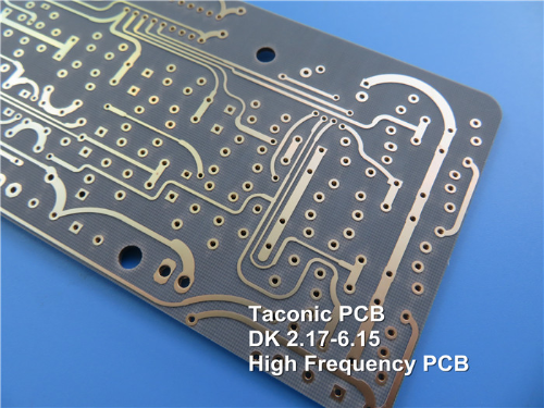
Founded in 2003, Shenzhen Bicheng Electronics Technology Co., Ltd is an established high frequency PCB supplier and exporter in Shenzhen, China, serving customers worldwide.
We are devoted to delivering high-frequency PCB products and solutions of the highest quality, along with customized service. Feel free to consult and contant at any time !
Visit https://www.bicheng-enterprise.com to learn more.
Unlock its full potential by contacting Vicky at v.xie@bichengpcb.com. |
|
|
| |
|
|
|
|
| |
|
|
|
|
| |
|
|
|
|
| |
|
|
|
| |
|
|
|
| |
|
|
|
|
|