| |
 |
| |
|
|
|
|
|
| |
|
What is Minimum Space in High Frequency PCB? |
|
|
|
| |
|
1. Definition of Minimum Trace Width |
|
|
|
| |
|
Minimum Space refers to the minimum distance between adjacent copper traces, adjacent pads, or between pads and traces, typically measured in mils or millimeters. |
|
|
| |
|
|
|
|
| |
|
2. Factors Affecting Minimum Space |
|
|
| |
|
2.1 Signal Crosstalk Smaller spacing increases the risk of crosstalk due to electromagnetic field coupling, especially in high-frequency or high-speed digital circuits. Analog signals are more sensitive to crosstalk than digital signals, requiring larger spacing in mixed-signal PCB designs.
2.2 Manufacturing Process and Cost
Smaller spacing demands higher manufacturing precision, increasing the risk of defects (e.g., shorts) and production costs, especially in HDI PCB fabrication. Excessively small spacing can lower yield rates, requiring a balance between spacing and cost.
2.3 Insulation and Voltage Requirements
High-voltage circuits require sufficient spacing to prevent insulation breakdown or arcing. minimum space depends on insulation material properties and operating voltage to ensure safety and reliability. |
|
|
| |
|
|
|
|
| |
|
3.Measures to Increase minimum space |
|
|
| |
|
3.1 Rational Wiring
Use Differential Signals: Reduces crosstalk through electromagnetic field cancellation, commonly used in high-speed serial communication.
Adjust Wiring Directions: Minimize parallel wiring; use vertical or diagonal crossings to reduce interference.
3.2 Enhance Insulation
Better Substrate Materials: Use materials with low dielectric constants and good insulation to prevent crosstalk and breakdown.
Thicker Insulation Layers: Increase solder mask thickness to improve insulation while balancing signal speed.
3.3 Partitioning and Shielding
Signal Partitioning: Separate analog/digital or high/low voltage signals with isolation zones or shielding layers. For example, In audio amplifiers, isolate small-signal inputs from high-voltage areas for flexible spacing.
|
|
|
| |
|
|
|
|
| |
|
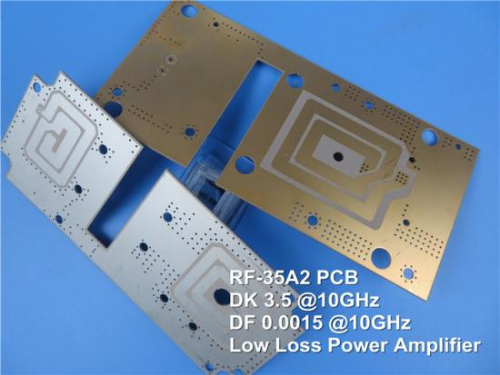
4.Strengths of Rogers RF - 35A2 PCB's Minimum Space |
|
|
| |
|
When it comes to minimum space in PCBs, I invariably think of Rogers RF - 35A2 high-frequency PCB. Let's delve into the key details of this remarkable product. |
|
|
| |
|
|
|
|
| |
|
 |
|
|
| |
|
|
|
|
| |
|
4.1 Signal Transmission |
|
|
| |
|
Low Dielectric Constant:
With a DK of 3.5 ± 0.05, RF-35A2 is ideal for high-frequency circuits, enabling faster signal travel and longer wavelengths. This allows for meeting electrical length needs in less space, reducing PCB size and permitting closer line spacing. For a 5 GHz microstrip line, it shortens the line, accommodating more components and minimizing gaps.
Low Loss Factor:
DF of 0.0015 effectively reduces signal attenuation and distortion in high-frequency applications, maintaining high signal quality and low crosstalk even with narrow line spacing. Compared to higher-loss materials, it allows for reliable signaling in smaller spaces without necessitating wider spacing to prevent interference. |
|
|
| |
|
|
|
|
| |
|
4.2 Manufacturing Precision |
|
|
| |
|
Dimensional Stability:
The glass fiber cloth in RF-35A2 laminate ensures dimensional stability during production, resisting changes from heat and moisture. This guarantees accurate line spacing, particularly for fine lines and multilayer boards. For 0.1 mm-spaced lines, it maintains spacing integrity, reducing errors and supporting tight designs.
Fine Line Capability:
RF-35A2 substrate can fabricate extremely fine lines and small spacings. Its smooth surface and strong copper foil bond enable precise control of line width and spacing in lithography and etching, achieving a line-width-to-spacing ratio of 1:1 or less. It can produce high-density lines that are 0.05 mm wide and spaced, allowing for more circuit functions in a compact area. |
|
|
| |
|
|
|
|
| |
|
4.3 Thermal Traits |
|
|
| |
|
High Thermal Conductivity:
Efficiently conducts heat away from hot components. In high-frequency circuits with significant heat generation, good thermal management prevents swelling and performance degradation, ensuring stable PCB and line spacing. In a power amplifier PCB, it dissipates heat quickly, maintaining small spacings at high power and preventing short circuits from heat-induced shrinkage.
Matched Thermal Expansion:
The X and Y axes of RF-35A2 PCB are 10 ppm/°C and 13 ppm/°C, respectively, close to that of copper. This small difference minimizes stress and warping during temperature changes, securing line spacing stability and allowing for tighter designs without large thermal expansion margins. |
|
|
| |
|
|
|
|
| |
|
5. RF - 35A2 vs. F4BTMS265: Minimum Space Advantages |
|
|
| |
|
Similarly, Wangling F4BTMS220 is also used in products with high - frequency signal transmission requirements. Let's examine the comparison of their advantages in minimum space. |
|
|
| |
|
|
|
|
| |
|
Items |
Rogers RF - 35A2 |
Wangling F4BTMS265 |
Dielectric Constant |
3.5 ± 0.05, faster signal propagation, shorter length for same elec. spec, aids compact layout & min. spacing reduction. |
2.65±0.04,
even faster signal propagation, may need more space for same elec. spec. |
Loss Factor |
0.0015at 10 GHz, small signal attenuation & distortion, low crosstalk at close spacing, facilitates tight layout. |
0.0012 at 10GHz, 0.0014 at 20GHz, 0.0018 at 40GHz, RF - 35A2 has clearer advantage at high frequencies. |
Thermal Expansion Coefficient |
X & Y axes are 10ppm/°C and 13ppm/°C that close to copper's, minor planar thermal expansion diff., enables precise spacing control in temp. changes. |
low CTE., but higher than RF - 35A2's. Weaker in spacing control during temp. |
Manufacturing Process Precision |
High surface flatness and strong copper foil adhesion, can reach 1:1 or narrower line-width/spacing, with good dimensional stability and thermal expansion match for precise control. |
Ultra-thin & ultra-fine glass fiber cloth reinforced, has lower tolerance & consistency, shows fine-line mfg. potential but weak in fine structure and thermal expansion spacing control. |
|
|
|
| |
|
|
|
|
| |
|
As can be analyzed from the above table,RF - 35A2 laminate has advantages in signal propagation, low loss factor, precise thermal expansion control and high manufacturing precision; while Wangling F4BTMS220 PCB has faster signal propagation but may need more space, has varying loss factors at different frequencies where RF - 35A2 PCB is better at high frequencies, and is weaker in spacing control and fine structure. |
|
|
| |
|
|
|
|
| |
|
6. Concluding Remarks |
|
|
| |
|
In PCB design, minimum space impacts performance & reliability. “Small spaces, big impacts.” Trace spacing affects signal interference; small space may boost crosstalk, degrading signal, while proper space cuts it. In high - frequency applications,it’s especially critical as freq rises. Also, it influences manufacturability; too small a space hikes defect risks, reasonable one aids production. |
|
|
| |
|
|
|
|
| |
|
Founded in 2003, Shenzhen Bicheng Electronics Technology Co., Ltd is an established high frequency PCB supplier and exporter in Shenzhen, China, serving customers worldwide.
We are devoted to delivering high-frequency PCB products and solutions of the highest quality, along with customized service. Feel free to consult and contant at any time !
Visit https://www.bicheng-enterprise.com to learn more.
Unlock its full potential by contacting Vicky at v.xie@bichengpcb.com. |
|
|
| |
|
|
|
|
| |
|
|
|
|
| |
|
|
|
|
| |
|
|
|
| |
|
|
|
| |
|
|
|
|
|