| |
 |
| |
|
|
|
|
|
| |
|
What is Lead-Free Process Compatible in High Frequency PCB? |
|
|
|
| |
|
1. Meaning of Lead-Free Process Compatible |
|
|
|
| |
|
In the manufacturing process of high-frequency PCBs, Lead-Free Process Compatible means not using lead-containing materials. Instead, appropriate lead-free materials and processes are selected to enable the PCBs to meet the performance requirements of high-frequency applications while conforming to environmental protection standards. |
|
|
| |
|
|
|
|
| |
|
2. Advantages of Lead-Free Process Compatible |
|
|
| |
|
2.1 Environmental Protection: Reduces lead pollution, meeting sustainable development needs.
2.2 Stable Performance: Ensures stable electrical performance with suitable lead-free materials and processes.
2.3 Compliance with Regulations: Satisfies strict environmental regulations and avoids legal risks.
2.4 Brand Image Enhancement: Demonstrates environmental commitment and boosts brand competitiveness. |
|
|
| |
|
|
|
|
| |
|
3. Significance of Lead-Free Process |
|
|
| |
|
3.1Crucial in Advanced Technologies:
Understanding Lead-Free Process Compatible is crucial in the realm of high frequency PCBs. High frequency PCBs are essential in advanced technologies like telecommunications (used in 5G base stations for reliable signal transmission) and aerospace.
3.2 Meeting Sustainable Demand:
Manufacturing without lead meets the growing demand for sustainable electronics. In the automotive industry (for ADAS and electric vehicle charging systems) and medical devices (diagnostic equipment and implantable devices), lead-free compatibility is vital for safety and regulatory compliance.
3.3 Material and Process Requirements:
It involves using materials and processes that can handle high temperatures and demanding requirements while ensuring reliable performance, like careful selection of materials with low dielectric loss and stable electrical properties.
3.4 Optimized Manufacturing Processes:
Optimized manufacturing processes for lead-free soldering and assembly create high-performance and environmentally friendly PCBs. Among various high frequency PCBs, Taconic TLX-8, which excels in lead-free process compatible, is the one I prefer to discuss. |
|
|
| |
|
|
|
|
| |
|
4. Taconic TLX-8 PCB: A Recommended Choice |
|
|
| |
|
Taconic TLX-8,high volume fiberglass reinforced microwave substrate,has high heat resistance and can withstand the high temperatures required in the lead-free soldering process. It also has an extremely low dielectric loss of 0.0018 at 10 GHz. Moreover, it possesses fine mechanical strength and stability. TLX-8 is a workhorse in the RF microwave substrate world. What's even more remarkable is that It has a proven track record in space applications and is utilized wherever woven fiberglass reinforcement is needed. |
|
|
| |
|
|
|
|
| |
|
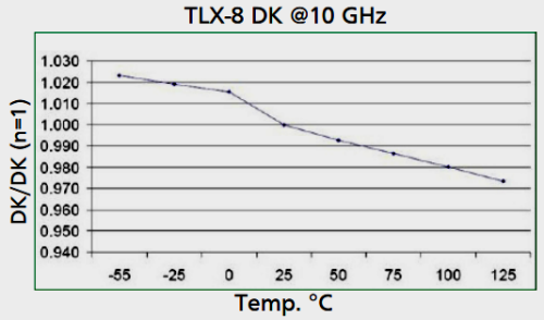
4-1. Thermal Coefficient of Taconic TLX-8 |
|
|
| |
|
 |
|
|
| |
|
|
|
|
| |
|
According to the above chart, it can be known that TLX-8 has a variation of approximately ±2% in DK from -55 to 125 °C, indicating stable Dk.
*Measurements were conducted using a manufactured PCB coupon with 20 watts per channel at 800 and 1800 MHz. |
|
|
| |
|
|
|
|
| |
|
4-2. Detailed Specifications for Taconic TLX-8 |
|
|
| |
|
|
|
|
| |
|
TLX-8 PCB Datasheet
PCB material: |
PTFE Fiberglass Laminates |
Designation: |
TLX-8 |
Dielectric constant: |
2.55 |
Layer count: |
Sinlge-sided PCB, Double-sided PCB, Multi-layer PCB, Hybrid PCB |
Dielectric thickness: |
2.5mil (0.0635mm), 10mil (0.254mm), 20mil (0.508mm), 25mil (0.635mm), 30mil(0.762mm), 50mil (1.27mm), 60mil (1.524mm), 75mil(1.905mm), 100mil (2.54mm), 125mil (3.175mm), 150mil (3.81mm), 200mil (5.08mm), 250mil (6.35mm) |
Copper weight: |
1oz (35µm), 2oz (70µm) |
PCB size: |
≤400mm X 500mm |
Solder mask: |
Green, Black, Blue, Red, Yellow etc. |
Surface finish: |
Immersion gold, HASL, Immersion silver, Immersion tin,Bare copper, OSP, ENEPIG, Pure gold etc.. |
|
|
|
| |
|
|
|
|
| |
|
4.1 Benefits of Taconic TLX-8 |
|
|
| |
|
• Excellent PIM Values in PCBs (measured at lower than -160 dBc*)
• Excellent Mechanical & Thermal Properties
• Low and Stable Dk
• Dimensionally Stable
• Low Moisture Absorption
• Tightly Controlled DK
• Low DF
• UL 94 VO Rating
• For Low Layer Count Microwave Designs |
|
|
| |
|
|
|
|
| |
|
4.2 Applications of Taconic TLX-8 |
|
|
| |
|
• Antennas
• Mixers, Splitters, Filters & Combiners
• Passive Components |
|
|
| |
|
|
|
|
| |
|
5. High-Frequency PCB Lead-Free Trends |
|
|
| |
|
5.1 Materials: Develop low-dielectric, low-loss, high-heat-resistance lead-free materials.
5.2 Surface Treatment: Innovate processes like ENIG, OSP for better solderability and oxidation resistance.
5.3 Equipment & Processes: Optimize welding equipment and processes. E.g., new reflow ovens, laser welding.
5.4 Reliability Research: Strengthen research on lead-free product reliability.
5.5 Green Integration: Integrate with green manufacturing concepts. |
|
|
| |
|
|
|
|
| |
|
6. Concluding Remarks |
|
|
| |
|
Overall, lead-free compatibility is essential for high frequency PCBs to meet environmental, performance, and regulatory requirements. In this regard,TLX-8 shows the path to embrace lead-free in high-frequency PCBs. |
|
|
| |
|
|
|
|
| |
|
Founded in 2003, Shenzhen Bicheng Electronics Technology Co., Ltd is an established high frequency PCB supplier and exporter in Shenzhen, China, serving customers worldwide.
We are devoted to delivering high-frequency PCB products and solutions of the highest quality, along with exceptional service ! |
|
|
| |
|
|
|
|
| |
|
|
|
|
| |
|
|
|
|
| |
|
|
|
| |
|
|
|
| |
|
|
|
|
|