| |
 |
| |
|
|
|
|
|
| |
|
What is LF-HASL in High Frequency PCB ? |
|
|
|
| |
|
1. Basic Principle |
|
|
|
| |
|
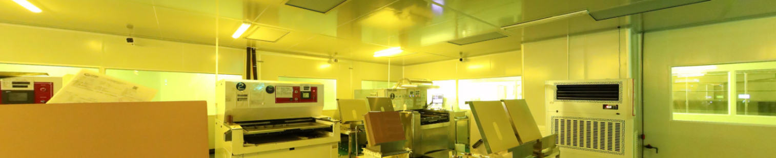
Lead-Free Hot Air Solder Leveling( LF-HASL)is widely used in high-frequency PCBs. It uses lead-free tin alloys (e.g., Sn-3.0Ag-0.5Cu) instead of traditional tin-lead ones. The process involves pretreating the PCB welding surface by chemical cleaning and other methods, placing it in equipment, melting the alloy, and spraying with high-pressure gas to form a uniform tin layer. |
|
|
| |
|
|
|
|
| |
|
2. Advantages |
|
|
| |
|
|
|
|
| |
|
2.1 Environmental Protection |
|
|
| |
|
LF-HASL avoids lead use in high-frequency PCB manufacturing, reducing environmental pollution risks. It complies with strict regulations like RoHS, helping products enter the international market.The investment in the research and development of lead-free tin alloys is to create a cleaner and healthier future for electronic manufacturing. |
|
|
| |
|
|
|
|
| |
|
2.2 Superior Performance |
|
|
| |
|
The tin layer has good solderability. Despite a higher melting point of lead-free alloys, optimized parameters ensure good welding. Lead-free solder joints are stable and have good anti-aging properties, improving product lifespan and reliability. LF-HASL PCB usually has a relatively smooth and bright surface, whereas the surface finish of Pb-HASL may be uneven. |
|
|
| |
|
|
|
|
| |
|
3. Limitations and Challenges |
|
|
| |
|
|
|
|
| |
|
3.1 Cost Aspect |
|
|
| |
|
The raw material cost of lead-free tin alloys is relatively high. The equipment and process are complex and need to be upgraded or replaced. The investment cost, maintenance cost, and energy consumption are also relatively high. With the development of modern electronic technology, the price difference between leaded and Lead-Free Hot Air Solder Leveling has become negligible. |
|
|
| |
|
|
|
|
| |
|
3.2 Process Compatibility |
|
|
| |
|
There may be compatibility issues between lead-free hot air solder leveling PCB and traditional processes, and the welding process parameters need to be adjusted. When converting old electronic product designs, PCB designs may need to be modified. |
|
|
| |
|
|
|
|
| |
|
3-1. Comparison between Pb-HASL and LF-HASL PCB
Comparison |
Lead-containing Hot Air Solder Leveling |
Lead-free Hot Air Solder Leveling |
Cost |
Lower |
High at first, now tiny |
Availability |
Widely available |
Readily available |
Reworkability |
Easy |
Possible with adjustments |
Shelf Life |
Certain shelf life |
Extended stability |
Environmental Impact |
Harmful |
Environmentally friendly |
Welding Performance |
Adequate |
Superior stability and anti-aging |
Process Compatibility |
Somewhat compatible |
Adjustments needed for improved compatibility |
|
|
|
| |
|
|
|
|
| |
|
4.Profile of Rogers RO4730G3 PCB |
|
|
| |
|
Among numerous high-frequency PCBs with LF-HASL , I prefer Rogers RO4730G3 Laminate that offers a cost-effective and technologically advanced solution for environmentally friendly manufacturing and assembly processes. RO4730G3 belongs to the RO4700™ series antenna grade laminates. It utilizes a ceramic-filled PTFE composite material and provides a reliable alternative to conventional PTFE-based laminates. Let's explore the specific information of RO4730G3. |
|
|
| |
|
|
|
|
| |
|
4.1 Technical Advantages: |
|
|
| |
|
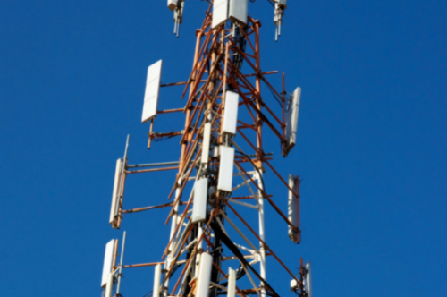
Antenna Design Properties
RO4730G3 laminate has the mechanical and electrical properties that antenna designers need. It has a dielectric constant of 3.0±0.5 (process), 2.98 (design) at 10GHz, and a loss factor as low as 0.0028 at 10 GHz /23℃ when using LoPro® Reverse Treated EDC Foil. These values allow antenna designers to realize substantial gain values while minimizing signal loss. It can also ensure the stability and accuracy of high-frequency signal transmission. |
|
|
| |
|
|
|
|
| |
|
 |
|
|
| |
|
|
|
|
| |
|
Low PIM & Temperature Stability
The RO4730G3 materials are available with a demonstrated low PIM performance, with values better than -160 dBc (43dBm 1,900MHz signal). It has stable performance in a wide temperature range and can adapt to various complex working environments. |
|
|
| |
|
|
|
|
| |
|
Thermal Conductivity & Plated Through Holes Reliability
RO4730G3 has excellent thermal conductivity of 0.45W/mk at 50℃. The glass transition temperature surpasses 280 ℃, resulting in a low CTE in the Z-axis and exceptional reliability of plated through holes. It is suitable for applications with high frequency, high temperature and high requirements for signal transmission quality. |
|
|
| |
|
|
|
|
| |
|
Flammability Rating
The RO4730G3 material has attained a flammability rating of V-0, conforming to the stringent standards of UL 94. This rating signifies its self-extinguishing capabilities and excellent resistance to combustion. |
|
|
| |
|
|
|
|
| |
|
4.2 Price Advantage |
|
|
| |
|
Compared to other high-frequency PCBs, RO4730G3 is relatively affordable. |
|
|
| |
|
|
|
|
| |
|
4-2. 4730G3 Datasheet |
|
|
| |
|
PCB Material: |
Hydrocarbon ceramic woven glass |
Designation: |
RO4730G3 |
Dielectric constant: |
3.0 ±0.05 (process) |
|
2.98 (design) |
Layer count: |
1-layer, 2-layer, Multi-layer, Hybrid designs |
Laminate thickness (low profile copper): |
5.7mil(0.145mm), 10.7mil(0.272mm), 20.7mil(0.526mm, 30.7mil(0.780mm), 40.7mil(1.034mm), 60.7mil(1.542mm) |
Laminate thickness (ED Copper): |
20mil(0.508mm), 30mil(0.762mm), 40mil(1.016mm), 50mil(1.270mm), 60mil(1.524mm) |
Copper weight: |
1oz (35 µm), 2oz (70µm) |
PCB size: |
≤400mm X 500mm |
Solder mask: |
Green, Black, Blue, Yellow, Red etc. |
Surface finish: |
Immersion gold, HASL, Immersion silver, Immersion tin, Bare copper, OSP, Pure gold, ENEPIG etc. |
|
|
|
| |
|
|
|
|
| |
|
5.Recap |
|
|
| |
|
Lead-free hot air solder leveling PCBs offer several advantages: environmental friendliness, harmlessness to human health, excellent performance, and superior appearance quality. Choosing LF-HASL is an investment for the future of the earth and human health. |
|
|
| |
|
|
|
|
| |
|
Founded in 2003, Shenzhen Bicheng Electronics Technology Co., Ltd is an established high frequency PCB supplier and exporter in Shenzhen, China, serving customers worldwide.
We are devoted to delivering high-frequency PCB products and solutions of the highest quality, along with exceptional service. Feel free to consult and contant at any time ! |
|
|
| |
|
|
|
|
| |
|
|
|
|
|
| |
|
|
|
|
|
| |
|
|
|
| |
|
|
|
| |
|
|
|
|
|