| |
 |
| |
|
|
|
|
|
| |
|
What is EMI Interference in High Frequency PCB ? |
|
|
|
| |
|
1. Understanding EMI Interference |
|
|
|
| |
|
IEMI Interference (Electromagnetic Interference) refers to the disruption caused by electromagnetic energy generated by electronic devices or systems during operation, which adversely affects the performance or functionality of other devices or systems. In the design of high-frequency PCBs, EMI interference is a critical concern because high-frequency signals are more prone to radiation and coupling, leading to potential interference issues. |
|
|
| |
|
|
|
|
| |
|
2.Core Hazards of EMI to High-Frequency PCBs |
|
|
| |
|
Signal Integrity Degradation: High-frequency signals distorted by EMI lead to data transmission errors or interruptions (e.g., USB/HDMI signal loss).
Circuit Malfunction: Sensitive analog circuits have abnormal outputs, and digital circuits may trigger wrong logic (e.g., counter miscounting).
EMC Failure: Excessive PCB radiation causes product to fail EMC certification, preventing market sales.
Shorter Equipment Lifespan: Long-term high-frequency interference accelerates component aging, causing intermittent failures.
Safety Hazards: Strong EMI may cause insulation breakdown and short circuits, risking fire or electric shock. |
|
|
| |
|
|
|
|
| |
|
3.Methods to Deal with EMI |
|
|
| |
|
3.1 Layout and Wiring For high-speed signal lines, keep them short and straight, avoid parallel arrangement, and use fewer right angles and acute angles. For RF (radio frequency) lines, adopt appropriate forms and ensure impedance matching. Place high-frequency and sensitive components away from interference sources, and put components prone to interference at the edge of the PCB and shield them. 3.2 Power and Ground Plane Design Use a complete ground plane to provide a low-impedance return path for signals, reducing radiation and coupling. Place the power plane adjacent to the ground plane, and utilize the parasitic capacitance to provide high-frequency bypassing and reduce power noise. 3.3 Shielding and Filtering Use shielded cables or add shielding layers on the PCB for sensitive or high-frequency signals. For example, use a shielding cover for audio circuits. Use LC or π-shaped filters for power lines, and RC filters or beads for signal lines to filter out high-frequency noise.
|
|
|
| |
|
|
|
|
| |
|
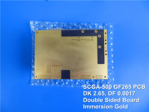
4.SCGA-500 GF265 PCB Material for EMI Reduction and Signal Stability |
|
|
| |
|
Engineered to meet the demands of modern RF/microwave design platforms, Shengyi SCGA-500 GF265 Hybrid PCB is a high-performance, low-loss PTFE woven glass material with UL 94 V-0 flammability rating. |
|
|
| |
|
|
|
|
| |
|
|
|
|
| |
|
 |
|
|
| |
|
|
|
|
| |
|
4.1 Low dielectric constant: |
|
|
| |
|
SCGA-500 GF265 PCB has a dielectric constant of 2.65±0.04, enabling fast signal transmission and small signal delay. This reduces phase differences, minimizing signal interference and EMI. |
|
|
| |
|
|
|
|
| |
|
4.2 Low dissipation factor: |
|
|
| |
|
SCGA-500 GF265 laminate features a dissipation factor of 0.0017, ensuring minimal energy loss at high frequencies. This maintains excellent signal integrity with low distortion, reducing EMI caused by signal distortion. |
|
|
| |
|
|
|
|
| |
|
4.3 Coefficient of thermal expansion (CTE): |
|
|
| |
|
SCGA-500 GF265 substrate exhibits a CTE of 9.2 in the X/Y-axis and 8.8/18 in the Z-axis. Its proper CTE reduces PCB deformation due to temperature changes, avoiding EMI caused by structural deformation. |
|
|
| |
|
|
|
|
| |
|
4.4 High resistivity: |
|
|
| |
|
SCGA-500 GF265 PCB boasts a volume resistivity of 1.2×10⁸ and a surface resistivity of 1.3×10⁸. Its high resistivity suppresses leakage current, effectively reducing EMI caused by electrical leakage. |
|
|
| |
|
|
|
|
| |
|
4.5 Peel strength: |
|
|
| |
|
SCGA-500 GF265 substrate offers a peel strength of 1.2 [6.86], ensuring strong inter-layer bonding. This enhances the structural stability of the PCB, reducing inter-layer electromagnetic coupling and EMI. |
|
|
| |
|
|
|
|
| |
|
4.6 Low water absorption: |
|
|
| |
|
GF265 laminate has a water absorption rate of 0.007, ensuring stable electrical properties even in humid environments. This reduces EMI caused by changes in humidity. |
|
|
| |
|
|
|
|
| |
|
4-1. SCGA-500 GF265 PCB Datasheet |
|
|
| |
|
PCB Capability (SCGA-500 GF265) |
PCB Material: |
PTFE Woven Glass |
Designation: |
SCGA-500 GF265 |
Dielectric constant: |
2.65 (10 GHz) |
Dissipation factor |
0.0017 (10 GHz) |
Layer count: |
Double Sided PCB, Multilayer PCB, Hybrid PCB |
Copper weight: |
1oz (35µm), 2oz (70µm) |
Dielectric thickness |
10mil (0.254mm), 20mil (0.508mm), 30mil (0.762mm), 40mil (1.016mm), 50mil (1.270mm), 60mil (1.524mm) |
PCB size: |
≤400mm X 500mm |
Solder mask: |
Green, Black, Blue, Yellow, Red etc. |
Surface finish: |
Bare copper, HASL, ENIG, Immersion silver, Immersion tin, OSP, Pure gold plated etc.. |
|
|
|
| |
|
|
|
|
| |
|
5.Takeaways |
|
|
| |
|
In high-frequency PCBs, EMI countermeasures are like calibrators of precision instruments, accurately regulating the electromagnetic environment, ensuring that every signal can travel purely and efficiently within the circuits. They become the decisive factor in determining the quality and competitiveness of electronic products and serve as the core driving force for the continuous innovation of the industry. |
|
|
| |
|
|
|
|
| |
|
Founded in 2003, Shenzhen Bicheng Electronics Technology Co., Ltd is an established high frequency PCB supplier and exporter in Shenzhen, China, serving customers worldwide.
We are devoted to delivering high-frequency PCB products and solutions of the highest quality, along with customized service. Feel free to consult and contant at any time !
Visit https://www.bicheng-enterprise.com to learn more.
Unlock its full potential by contacting Vicky at v.xie@bichengpcb.com. |
|
|
| |
|
|
|
|
| |
|
|
|
|
| |
|
|
|
|
| |
|
|
|
| |
|
|
|
| |
|
|
|
|
|