| |
 |
| |
|
|
|
|
|
| |
|
What is Coupler in High Frequency PCB? |
|
|
|
| |
|
1. Meaning of Coupler |
|
|
|
| |
|
A coupler is a passive device in high-frequency PCB design that transfers electromagnetic energy between circuits, enabling functions like signal splitting, combining, or sampling. Key types include directional couplers (for signal sampling and power measurement), hybrid couplers (for phase-shifting and balanced amplifiers), power dividers/combiners (for antenna arrays), and RF splitters (for communication systems). |
|
|
| |
|
|
|
|
| |
|
2. Key Characteristics of Couplers |
|
|
| |
|
2.1 Coupling Factor
The ratio of the coupled signal to the input signal, typically expressed in dB.
2.2 Directivity
The ability to isolate the forward and backward signals, indicating the coupler's efficiency.
2.3 Insertion Loss
The amount of signal loss when passing through the coupler.
2.4 Frequency Range
The operational bandwidth of the coupler, which must match the application's frequency requirements.
2.5 Isolation
The degree of separation between the input and output ports, ensuring minimal interference. |
|
|
| |
|
|
|
|
| |
|
3. Applications of Couplers in High-Frequency PCBs |
|
|
| |
|
3.1 Signal Monitoring
Sampling a portion of the signal for analysis or feedback without disrupting the main signal path.
3.2 Power Distribution
Splitting or combining signals in RF systems, such as antenna arrays or transceivers.
3.3 Impedance Matching
Ensuring efficient energy transfer between circuits with different impedance levels.
3.4 Phase Shifting
Creating phase differences for applications like beamforming in radar systems.
3.5 Test and Measurement
Used in network analyzers and other test equipment to measure signal strength and quality. |
|
|
| |
|
|
|
|
| |
|
4. Advantages of F4BME233 PCB in Couplers |
|
|
| |
|
Wangling F4BME series PCBs, crafted with a scientific blend of fiberglass cloth, PTFE resin, and PTFE film under strict quality control, offer distinct advantages when applied in couplers. We'll take Wangling F4BME233 PCB as an example for a comprehensive explanation.
4.1 Dielectric Properties
The dielectric constant of F4BME233 laminate is 2.33 at 10GHz with a tolerance of ±0.04. When applied in couplers, it enables precise control of the signal phase and amplitude, ensuring accurate power distribution and reducing signal distortion and interference.
The loss tangent is 0.0011 at 10GHz and 0.0015 at 20GHz, which reduces signal - transmission losses, improves the signal - transmission efficiency of the coupler, and is suitable for high - frequency communication systems.
4.2 Thermal Properties
The coefficient of thermal expansion is 2230ppm/℃ in the XY direction and 205ppm/℃ in the Z direction. When the coupler generates heat during operation, it can prevent structural damage caused by inconsistent thermal expansion and contraction, ensuring stable performance.
The temperature coefficient of the dielectric constant is - 130PPM/℃ ( - 55℃ - 150℃), which allows the coupler to maintain a stable operating state under different temperatures and adapt to complex environments.
4.3 Mechanical Properties
The peel strength of 1OZ F4BME is greater than 1.6N/mm, ensuring a firm connection between layers and between components and the board during the manufacture of the coupler, preventing delamination or component detachment, and improving mechanical reliability.
4.4 Electrical Properties
The volume resistivity is ≥6×10⁶MΩ.cm, and the surface resistivity is ≥1×10⁶MΩ, which can prevent current leakage and short - circuits in the coupler, ensuring the purity and integrity of the signals.
The electrical strength in the Z direction is greater than 23KV/mm, and the breakdown voltage in the XY direction is greater than 32KV, enabling the coupler to withstand high voltages and avoid electrical breakdown, ensuring safe operation.
4.5 Thermal Stress Properties
No delamination was observed during the test at 260℃ for 10 seconds, 3 times. This ensures the structural and performance stability of the coupler during the thermal cycles of soldering and use, and extends its service life. |
|
|
| |
|
|
|
|
| |
|
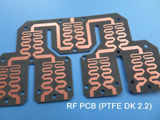
4-1. F4BME PCB |
|
|
| |
|
 |
|
|
| |
|
|
|
|
| |
|
5.Typical Applications |
|
|
| |
|
Microwave, RF, radar
Phase shifter, passive components
Power divider, coupler and combiner
Feed network, phased array antenna
Satellite communication, base station antenna |
|
|
| |
|
|
|
|
| |
|
5-1. Our PCB Capability(F4BME) |
|
|
| |
|
PCB Capability (F4BME) |
PCB Material: |
PTFE glass fiber cloth copper clad laminates |
Designation (F4BME ) |
F4BME |
DK (10GHz) |
DF (10 GHz) |
|
F4BME217 |
2.17±0.04 |
0.0010 |
|
F4BME220 |
2.20±0.04 |
0.0010 |
|
F4BME233 |
2.33±0.04 |
0.0011 |
|
F4BME245 |
2.45±0.05 |
0.0012 |
|
F4BME255 |
2.55±0.05 |
0.0013 |
|
F4BME265 |
2.65±0.05 |
0.0013 |
|
F4BME275 |
2.75±0.05 |
0.0015 |
|
F4BME294 |
2.94±0.06 |
0.0016 |
|
F4BME300 |
3.00±0.06 |
0.0017 |
Layer count: |
Single Sided, Double Sided PCB, Multilayer PCB, Hybrid PCB |
Copper weight: |
0.5oz (17 µm), 1oz (35µm), 2oz (70µm) |
Dielectric thickness
(or overall thickness) |
0.127mm (dielectric), 0.2mm, 0.25mm, 0.5mm, 0.508mm, 0.762mm, 0.8mm, 1.0mm, 1.5mm, 1.524mm, 1.575mm, 2.0mm, 2.5mm, 3.0mm, 4.0mm, 5.0mm, 6.0mm, 8.0mm, 10.0mm, 12.0mm |
PCB size: |
≤400mm X 500mm |
Solder mask: |
Green, Black, Blue, Yellow, Red etc. |
Surface finish: |
Bare copper, HASL, ENIG, Immersion silver, Immersion tin, OSP, Pure gold, ENEPIG etc.. |
|
|
|
| |
|
|
|
|
| |
|
6. Summary |
|
|
| |
|
Couplers are not only the bridges that connect physical components, but also the crucial hubs for the smooth flow of data and signals. With their exquisite design and outstanding performance, they underpin the efficient operation of modern technology. |
|
|
| |
|
|
|
|
| |
|
Founded in 2003, Shenzhen Bicheng Electronics Technology Co., Ltd is an established high frequency PCB supplier and exporter in Shenzhen, China, serving customers worldwide.
We are devoted to delivering high-frequency PCB products and solutions of the highest quality, along with customized service. Feel free to consult and contant at any time !
Visit https://www.bicheng-enterprise.com to learn more.
Unlock its full potential by contacting Vicky at v.xie@bichengpcb.com. |
|
|
| |
|
|
|
|
| |
|
|
|
|
| |
|
|
|
|
| |
|
|
|
| |
|
|
|
| |
|
|
|
|
|
|