| |
 |
| |
|
|
|
|
|
| |
|
What is Break-away Hole in High Frequency PCB? |
|
|
|
| |
|
1. Definition and Function of Break-away Holes |
|
|
|
| |
|
In high-frequency PCB design, a Break-away hole is a specialized hole that ensures signal integrity. It enables effective connections on multilayer boards and allows for easy disconnection during assembly, enhancing flexibility and maintainability. By optimizing the size and position of these holes, designers can minimize signal loss and improve performance, making them crucial for high-frequency applications. |
|
|
| |
|
|
|
|
| |
|
2. Guidelines for Selecting Break-away Holes |
|
|
| |
|
2.1 Size Selection Principles
When selecting the size of Break-away holes, several factors need to be considered:
Hole Diameter: For high-frequency signals, it is generally recommended to use smaller diameters to reduce parasitic inductance and capacitance; larger currents may require an increase in diameter to ensure effective conduction.
Mechanical Strength: Choose an appropriate diameter and wall thickness to ensure the hole's stability under mechanical stress and to prevent breakage.
Manufacturing Tolerances: The selected diameter should ensure that the required precision can be achieved during actual manufacturing.
2.2 Position Selection Principles
Position selection should follow these guidelines:
Layout Optimization: Place Break-away holes close to signal sources and loads to reduce the length of the signal transmission path.
Avoid Cross-Interference: Design should avoid placing holes in areas where signal lines cross to minimize the risk of signal interference.
Thermal Management: In high-power applications, the position of the holes should consider heat distribution to ensure effective heat dissipation.
Inter-layer Connections: In multilayer circuit boards, the position of the holes should match inter-layer connection requirements to ensure good electrical connectivity. |
|
|
| |
|
|
|
|
| |
|
3. High-Frequency Applications of Break-away Holes |
|
|
| |
|
The table shows the application fields of Break-away holes and their functions in various areas.
Application Field |
Description |
Wireless Communication Devices |
Used to connect antennas and RF components to ensure stable signal transmission. |
Automotive Radar Systems |
Connect radar sensors to signal processing units for precise object detection. |
Satellite Communication |
Connect high-frequency amplifiers to antennas to ensure signal integrity. |
RF Amplifiers |
Optimize the connections of internal components and reduce signal loss. |
Medical Equipment |
Connect sensors to signal processing circuits to ensure the transmission of high-frequency signals. |
Data Centers and Communication Base Stations |
Connect different layers of circuit boards to enhance the speed and reliability of data processing. |
Drones and Unmanned Aerial Vehicles |
Connect critical components to support real-time data transmission. |
Audio Equipment |
Ensure the integrity of audio signals and optimize the quality of wireless audio transmission. |
|
|
|
| |
|
|
|
|
| |
|
4. General Introduction of Rogers RO3003G2 |
|
|
| |
|
Of all the Rogers PCBs, I consider that the RO3003G2 PCB stands out the most in the design and application of Break-away Holes.
As an upgraded version of RO3003, RO3003G2 laminate further optimizes the resin and filler system, resulting in lower insertion loss. The material and structure are more uniform, reducing dielectric porosity, and its dielectric constant is stable at DK 3.00 at 10 GHz. The advanced filler system better supports microhole designs in Break-away Holes, meeting the high precision requirements for next-generation millimeter-wave automotive radar applications. |
|
|
| |
|
|
|
|
| |
|
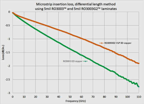
4-1.Comparison of Microstrip Insertion Loss |
|
|
| |
|
 |
|
|
| |
|
|
|
|
| |
|
In addition, RO3003G2 high frequency PCB uses very low profile (VLP) ED copper foil with minimal surface roughness. Compared to RO3003, it has even lower loss, with an insertion loss of only 1.3 dB/inch measured at 77 GHz using the microstrip differential phase length method on 5 mil thick material. |
|
|
| |
|
|
|
|
| |
|
5.Typical Applications of Rogers RO3003G2 |
|
|
| |
|
The following are the typical applications of Rogers RO3003G2:
Forward Collision Warning
Adaptive Cruise Control
Active Brake Assistance
Lane Change Assistance
Parking pilot
Traffic Jam pilot
Blind Spot Detection |
|
|
| |
|
 |
|
|
| |
|
|
|
|
| |
|
5-1. RO3003G2 Datasheet |
|
|
| |
|
PCB Capability (RO3003G2) |
PCB Material: |
Ceramic-filled PTFE Laminates |
Dielectric constant: |
3 |
Dissipation factor |
0.0011 |
Layer count: |
Single Sided, Double Sided, Multi-layer PCB, Hybrid PCB |
Copper weight: |
1oz (35µm), 2oz (70µm) |
Dielectric thickness |
5mil (0.127mm), 10mil (0.254mm) |
PCB size: |
≤400mm X 500mm |
Solder mask: |
Green, Black, Blue, Yellow, Red etc. |
Surface finish: |
Immersion gold, HASL, Immersion silver, Immersion tin, ENEPIG, OSP, Bare copper, Pure gold etc.. |
|
|
|
| |
|
|
|
|
| |
|
6. Conclusion |
|
|
| |
|
As an important element in high-frequency PCB design, Break-away holes hold a crucial position in enhancing circuit performance, simplifying layouts, and increasing design flexibility. With the continuous advancement of electronic technology, the application of Break-away holes will become increasingly widespread, helping engineers advance in innovation and design.
Founded in 2003, Shenzhen Bicheng Electronics Technology Co., Ltd is an established high frequency PCB supplier and exporter in Shenzhen, China, serving customers worldwide.
We are devoted to delivering high-frequency PCB products and solutions of the highest quality, along with customized service. Feel free to consult and contant at any time ! |
|
|
| |
|
|
|
|
| |
|
|
|
|
| |
|
|
|
|
| |
|
|
|
| |
|
|
|
| |
|
|
|
|
|