| |
 |
| |
|
|
|
|
|
| |
|
What is Board Tooling Hole in High Frequency PCB ? |
|
|
|
| |
|
1. Definition and Purpose of Board Tooling Hole |
|
|
|
| |
|
In high frequency printed circuit boards, the board tooling hole is a specialized feature that plays a crucial role. Specifically, it is a hole created during the manufacturing process to aid in production flow and ensure precision and alignment. Though it may seem like a small detail, it has a significant impact on achieving excellent performance and quality. |
|
|
| |
|
|
|
|
| |
|
2. Importance in High Frequency PCB Design |
|
|
| |
|
High frequency PCBs demand utmost signal integrity. The board tooling hole contributes to this by providing accurate placement and alignment of components. It helps in reducing signal distortion and interference. For example, when components are precisely aligned thanks to tooling holes, the signal paths are more stable, minimizing signal loss and crosstalk. |
|
|
| |
|
|
|
|
| |
|
3. Enhancing Signal Integrity with Board Tooling Hole |
|
|
| |
|
When we are enhancing signal integrity with board tooling hole, there are three aspects for us to consider.
Firstly, optimize the location. We should avoid setting the board tooling holes near high-speed signal lines. For key radio frequency signal paths, we should ensure the distance from the tooling hole is more than one-tenth of the signal wavelength. And we should also consider setting it in a low-sensitivity area considering the signal flow.
Secondly, adjust the size. We need to reduce the diameter as much as possible under the premise of meeting the requirements and optimize the board tooling holes to a circular or oval shape to reduce electromagnetic interference.
Thirdly, perform metallization treatment. This can enhance conductivity and electromagnetic shielding performance. As a result, signal transmission becomes smoother, attenuation is reduced, and external interference is resisted.
|
|
|
| |
|
|
|
|
| |
|
4. Rogers RO3006's Board Tooling Hole Superiorities |
|
|
| |
|
When discussing the application of board tooling holes in PCBs, Rogers RO3006 high frequency circuit board immediately comes to my mind.
RO3006 Rogers PCB boards are ceramic-filled PTFE composites,offering excellent thermal reliability and electrical performance at competitive prices. Let's examine the advantages of Rogers RO3006 PCBs regarding the design of board tooling holes. |
|
|
| |
|
|
|
|
| |
|
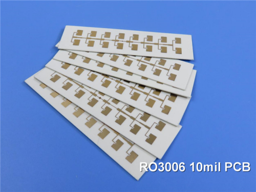
4-1. RO3006 10mil Rogers Substrate PCB |
|
|
| |
|
 |
|
|
| |
|
|
|
|
| |
|
4.1 Stability of High DK Ensures Signal Transmission Precision |
|
|
| |
|
RO3006 laminate has a dielectric constant of 6.15 ± 0.15 with high temperature and frequency stability. In Board Tooling Hole design, this stable dielectric constant guarantees signal precision and stability, reducing errors caused by environmental changes. It maintains signal quality even under large temperature variations or high frequencies, enhancing circuit reliability. |
|
|
| |
|
|
|
|
| |
|
4.2 Excellent Dimensional Stability Facilitates Precise Positioning |
|
|
| |
|
With a coefficient of thermal expansion(-55 to 288℃) of 17 ppm/°C in x and y directions (equivalent to copper) and 24 ppm/°C in z direction, RO3006™ shows excellent dimensional stability. This ensures accurate positioning of Board Tooling Hole during processing and in different temperatures, improving assembly accuracy and signal reliability. Suited for high-precision applications like automotive radars and GPS antennas. |
|
|
| |
|
|
|
|
| |
|
4.3 Low Dielectric Loss Boosts Signal Transmission Efficiency |
|
|
| |
|
Rogers 3006 PCB has a loss factor of 0.002 at 10 GHz. In Board Tooling Hole design, low dielectric loss reduces signal energy loss through holes, improving transmission efficiency and quality. Crucial for high-frequency signal transmission, it extends transmission distance and reduces attenuation, enhancing overall circuit performance. |
|
|
| |
|
|
|
|
| |
|
4-2. Other Specifications of RO3006 |
|
|
| |
|
Designation: |
RO3006 |
Layer count: |
2 Layer, Multilayer, Hybrid PCB |
Copper weight: |
0.5oz (17 µm), 1oz (35µm), 2oz (70µm) |
PCB thickness: |
10mil (0.254mm), 25mil (0.635mm) |
|
50mil (1.27mm) |
PCB size: |
≤400mm X 500mm |
Solder mask: |
Green, Black, Blue, Yellow, Red etc. |
Surface finish: |
Bare copper, HASL, ENIG, OSP etc.. |
|
|
|
| |
|
|
|
|
| |
|
5. Typical Applications |
|
|
| |
|
Automotive radar applications
Power amplifiers and antennas
GPS Antennas
Direct broadcast satellite
Patch antennas for wireless communications |
|
|
| |
|
|
|
|
| |
|
6. Summary |
|
|
| |
|
"The board tooling hole: A vital cog in the machinery of high frequency PCB production, driving excellence." |
|
|
| |
|
|
|
|
| |
|
Founded in 2003, Shenzhen Bicheng Electronics Technology Co., Ltd is an established high frequency PCB supplier and exporter in Shenzhen, China, serving customers worldwide.
We are devoted to delivering high-frequency PCB products and solutions of the highest quality, along with customized service. Feel free to consult and contant at any time !
Visit https://www.bicheng-enterprise.com to learn more.
Unlock its full potential by contacting Vicky at v.xie@bichengpcb.com. |
|
|
| |
|
|
|
|
| |
|
|
|
|
| |
|
|
|
|
| |
|
|
|
| |
|
|
|
| |
|
|
|
|
|