| |
|
|
|
|
|
|
|
|
Wangling TP PCB Thermoplastic Material with Wide Range DK 3.0-25 for Beidou and Miniaturized Antennas |
|
|
(Printed Circuit Boards are custom-made products. The picture and parameters shown are for reference only.) |
|
|
|
|
|
Brief Introduction |
|
|
Wangling TP PCB has emerged as a pioneering high-frequency thermoplastic in the PCB industry, distinguished by its innovative design and cutting-edge performance. The dielectric layer of its TP-type laminates integrates ceramics with polyphenylene Oxide resin (PPO), a composite structure that eliminates the need for traditional fiberglass reinforcement. What sets Wangling TP PCB apart is its unique ability to fine-tune the dielectric constant by simply altering the proportion of ceramics to PPO resin, offering engineers unprecedented flexibility in high-frequency circuit design.
Thanks to its specialized manufacturing process, Wangling TP PCB delivers superior dielectric performance and dependable reliability, making it a go-to solution for complex applications. The material’s naming system is intuitive and user-friendly: "TP" refers to the smooth-surfaced base material without copper cladding, "TP-1" indicates one-sided copper cladding, and "TP-2" signifies double-sided copper cladding. This straightforward labeling helps users quickly identify the right TP PCB variant for their project needs, enhancing its versatility across various industrial sectors. |
|
|
|
|
|
Features |
|
|
1.The TP material allows for the dielectric constant to be freely chosen within the 3 - 25 range, catering precisely to circuit demands. It maintains stability, with common values like 3.0, 4.4, 6.0, etc. Exhibiting low dielectric loss, though it rises with frequency, the change is minimal below 10 GHz.
2.Operating reliably from -100°C to +150°C, TP PCB excels in low - temperature resistance. But above 180°C, risks of material deformation, copper foil detachment, and electrical performance shifts emerge.
3.With a minimum thickness of 0.5mm, TP laminate offers multiple thickness options and can be customized to fit different application needs.
4.Resistant to radiation and featuring low outgassing, TP material ensures reliability in environments where these factors matter.
5.Ideal for applications like Beidou systems, missile - borne devices, fuzes, and miniaturized antennas, Wangling TP PCB meets the stringent requirements of these high - tech fields.
6. The copper foil adheres more dependably to the TP dielectric layer than to ceramic substrates with vacuum coating. It's easily machinable through drilling, turning, grinding, shearing, and etching, unlike ceramic substrates.
7. Simplifying PCB processing, TP material can be worked with thermoplastic - suitable methods, achieving high yields and cutting costs versus ceramic substrates. However, multilayer PCB processing isn't usually advisable; if needed, low - temperature bonding sheets should be used, and feasibility carefully evaluated. |
|
|
|
|
|
Data Sheet |
|
|
Product Technical Parameter |
Product Models & Data Sheet |
Product Features |
Test Conditions |
Unit |
TP TP-1 TP-2 |
Dielectric Constant |
When the dielectric constant is ≤11, the test condition is 10GHz.
When the dielectric constant is >11, the test condition is 5GHz. |
/ |
3.0±0.06 |
4.4±0.09 |
6.0±0.12 |
|
|
|
6.15±0.12 |
9.2±0.18 |
9.6±0.19 |
|
|
|
10.2±0.2 |
11.0±0.022 |
16.0±0.4 |
|
|
|
20.0±0.8 |
22.0±0.88 |
25.0±1.0 |
|
|
|
The dielectric constant can be customized within the range of 3.0 to 25. |
Dielectric Constant Tolerance |
Dielectric Constant 3.0Ұ«11.0 |
/ |
±2% |
|
Dielectric Constant 11.1Ұ«16.0 |
/ |
±2.5% |
|
Dielectric Constant 16.1Ұ«25.0 |
/ |
±4% |
Loss Tangent |
Loss Tangent 3.0Ұ«9.5 |
10GHz |
/ |
0.0010 |
|
Loss Tangent 9.6Ұ«11.0 |
10GHz |
/ |
0.0012 |
|
Loss Tangent 11.1Ұ«16.0 |
5GHz |
/ |
0.0015 |
|
Loss Tangent 16.1Ұ«25.0 |
5GHz |
/ |
0.0020Ұ«0.0025 |
Dielectric Constant Temperature Coefficient |
Dielectric Constant 3.0Ұ«9.5 |
-55 º~150ºC |
PPM/Ұж |
-50 |
|
Dielectric Constant 9.6Ұ«16.0 |
-55 º~150ºC |
PPM/Ұж |
-40 |
|
Dielectric Constant 16.1Ұ«25.0 |
-55 º~150ºC |
PPM/Ұж |
-55 |
Peel Strength |
1 OZ Normal State |
N/mm |
>0.6 |
|
1 OZ After AC Humidity Test |
N/mm |
>0.4 |
Volume Resistivity |
Normal State at 500V |
MΩ.cm |
>1×10⁹ |
Surface Resistivity |
Normal State at 500V |
MΩ |
>1×10⁷ |
Coefficient of Thermal Expansion
(XY Z) |
Dielectric Constant 3.00Ұ«4.40 |
-55 º~150ºC |
PPM/Ұж |
60,60,70 |
|
Dielectric Constant 4.60Ұ«6.15 |
-55 º~150ºC |
PPM/Ұж |
50,50,60 |
|
Dielectric Constant 6.16Ұ«11.0 |
-55 º~150ºC |
PPM/Ұж |
40,40,55 |
|
Dielectric Constant 11.1Ұ«16.0 |
-55 º~150ºC |
PPM/Ұж |
40,40,50 |
|
Dielectric Constant 16.1Ұ«25.0 |
-55 º~150ºC |
PPM/Ұж |
35,35,40 |
Water Absorption |
20±2Ұж, 24 hours |
% |
≤0.01 |
Long-Term Operating Temperature |
High-Low Temperature Chamber |
Ұж |
-100º~150ºC |
Material Composition |
Polyphenylene ether, ceramic, paired with ED copper foil. |
The density and thermal conductivity data for materials with different dielectric constants are as follows: |
Product Features |
Unit |
Dielectric Constanct |
|
|
3.0 |
4.4 |
6.0 |
6.15 |
9.6 |
10.2 |
11.0 |
16.0 |
20.0 |
22.0 |
25.0 |
Density |
g/cm3 |
1.69 |
1.89 |
2.1 |
2.12 |
2.26 |
2.33 |
2.40 |
2.76 |
2.73 |
2.77 |
2.94 |
Thermal Conductivity |
W/(M.K) |
0.40 |
0.44 |
0.55 |
0.55 |
0.65 |
0.67 |
0.70 |
0.80 |
0.85 |
0.90 |
1.0 |
|
|
|
|
|
|
 |
|
|
|
|
|
Our PCB Capability (TP Series) |
|
|
PCB Capability (TP Series) |
PCB Material: |
Polyphenylene ether, ceramic |
Designation (TP Series) |
Designation |
DK |
DF |
|
TP300 |
3.0±0.06 |
0.0010 |
|
TP440 |
4.4±0.09 |
0.0010 |
|
TP600 |
6.0±0.12 |
0.0010 |
|
TP615 |
6.15±0.12 |
0.0010 |
|
TP920 |
9.2±0.18 |
0.0010 |
|
TP960 |
9.6±0.2 |
0.0011 |
|
TP1020 |
10.2±0.2 |
0.0011 |
|
TP1100 |
11.0±0.22 |
0.0011 |
|
TP1600 |
16.0±0.32 |
0.0015 |
|
TP2000 |
20.0±0.4 |
0.0020 |
|
TP2200 |
22.0±0.44 |
0.0022 |
|
TP2500 |
25.0±0.5 |
0.0025 |
Layer count: |
Single Sided, Double Sided PCB |
Copper weight: |
1oz (35µm), 2oz (70µm) |
Dielectric thickness (Dielectric thickness or overall thickness) |
0.5mm, 0.8mm, 1.0mm, 1.2mm, 1.5mm, 2.0mm, 3.0mm, 4.0mm, 5.0mm, 6.0mm, 7.0mm, 8.0mm, 10.0mm, 12.0mm |
PCB size: |
≤150mm X 220mm |
Solder mask: |
Green, Black, Blue, Yellow, Red etc. |
Surface finish: |
Bare copper, HASL, ENIG, Immersion silver, Immersion tin, OSP, Pure gold, ENEPIG etc.. |
|
|
|
|
|
|
A TP PCB and Applications |
|
|
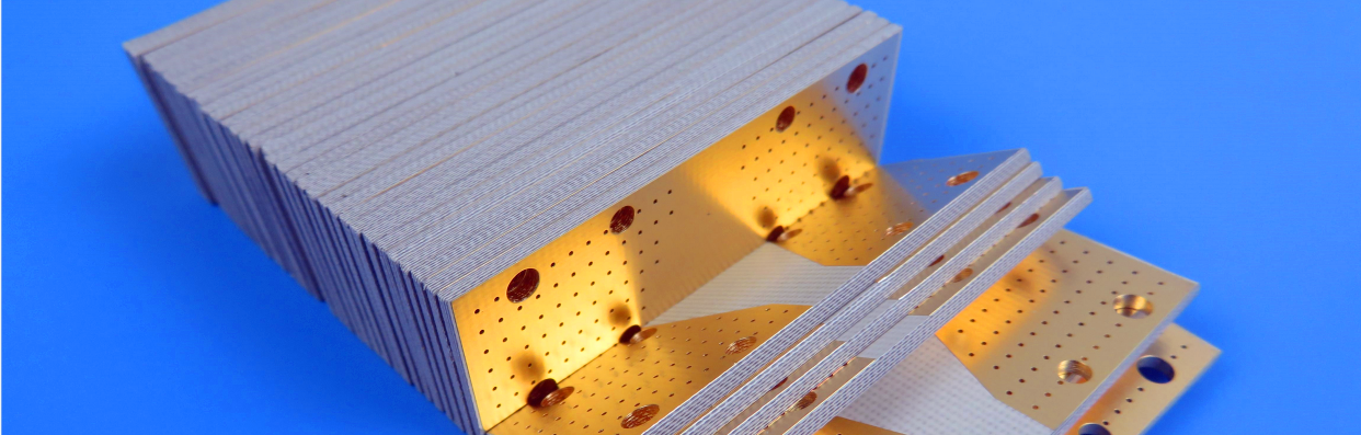
On the screen, you can see a 1.5mm TP high-frequency PCB with OSP (Organic Solderability Preservative) coating. TP high-frequency PCBs are also utilized in applications such as Beidou, missile-borne systems, fuzes, and miniaturized antennas. |
|
|
|
|
|
Final Attention |
|
|
When it comes to thermal and soldering processes, Wangling TP PCB presents distinct considerations that users should be aware of. Unlike some other PCB materials, Wangling TP PCB cannot endure thermal shock testing at 260°C, and wave soldering proves unsuitable for its unique composition. For effective soldering, relying on a constant - temperature soldering iron for hand soldering is the recommended method. While reflow soldering is generally not the preferred choice for TP laminate, in cases where it’s necessary, it’s essential to cap the temperature at a maximum of 200°C. Prior to attempting reflow soldering, a comprehensive evaluation of the process's feasibility and stability is imperative to safeguard the integrity of the TP material in TP PCB and ensure optimal performance of the final product. |
|
|
|
|
|
|
|
|
|
|
|
Hot Tags:
Wangling TP PCB |
Wangling TP Circuit Board |
TP-type laminate |
Antennas PCB |
High-frequency Thermoplastic PCB |
|
|
|