|
|
|
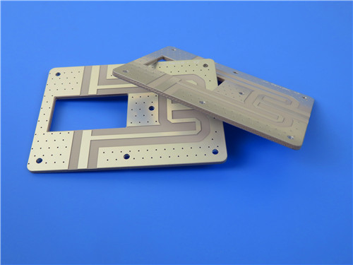
Taconic RF-10 Low Loss PCB Substrate 2-Layer 60mil with Immersion Tin for Optimal High Speed Signal Integrity |
|
|
|
|
|
|
|
1. Introduction of RF-10 PCB
Taconic RF-10 PCB combine ceramic-filled PTFE and woven fiberglass to deliver superior high-frequency performance. With a high dielectric constant and ultra-low dissipation factor, Taconic RF-10 PCB ensures minimal signal loss in demanding RF applications. The thin woven fiberglass reinforcement enhances rigidity for easier handling while maintaining excellent dimensional stability in multilayer designs.
Engineered for cost efficiency and fast industry-standard lead times, RF-10 Laminate enables compact RF circuit designs without compromising performance. Its exceptional bond with smooth, low-profile copper minimizes insertion losses—especially at high frequencies where skin effect dominates. This makes RF-10 PCB an ideal choice for high-speed, low-loss PCB applications requiring reliability and precision.
|
|
2. Features of RF-10 PCB
- Dielectric Constant of 10.2 ± 0.3 at 10GHz
- Dissipation Factor of 0.0025 at 10GHz
- High Thermal Conductivity of 0.85 W/mk (Unclad)
- x CTE of 16 ppm/°C, y CTE of 20 ppm/°C, z CTE of 25 ppm/°C
- Low Moisture Absorption of 0.08%
- Flammability Rating of V-0 |
|
|
|
3. Benefits of RF-10 PCB
- High DK for RF circuit size reduction
- Excellent dimensional stability
- Tight DK tolerance (10.2 +/- 0.3)
- High thermal conductivity for enhanced thermal management
- Excellent adhesion to smooth coppers
- Low X, Y, Z expansion
- Excellent price/performance ratio |
|
|
|
4. PCB Stackup: 2-layer rigid PCB
Copper_layer_1 - 35μm (1oz)
RF-10 Core - 60mil (1.524mm)
Copper_layer_2 - 35μm (1oz) |
|
| 5. PCB Construction Details: |
| |
| - Base material: RF-10
- Board dimensions: 64mm x 45.7mm=1PCS, +/- 0.15mm
- Minimum Trace/Space: 4/6 mils
- Minimum Hole Size: 0.4mm
- No Blind vias.
- Finished board thickness: 1.6mm
- Finished Cu weight: 1oz (1.4 mils) outer layers
- Via plating thickness: 20 μm
- Surface finish: Immersion tin
- Top Silkscreen: NO
- Bottom Silkscreen: No
- Top Solder Mask: NO
- Bottom Solder Mask: No
- 100% Electrical test used prior to shipment |
| |
|
 |
|
|
6. PCB Statistics:
Components: 26
Total Pads: 75
Thru Hole Pads: 43
Top SMT Pads: 32
Bottom SMT Pads: 0
Vias: 53
Nets: 2
|
|
|
|
7. Type of artwork supplied: Gerber RS-274-X |
|
|
|
8. Quality standard: IPC-Class-2 |
|
|
|
9. Availability: worldwide |
|
|
|
10. Typical Applications:
- Microstrip Patch Antennas
- GPS Antennas
- Passive Components (filters, couplers, power dividers)
- Aircraft Collision Avoidance Systems
- Satellite components |
|
|
|
|
|
|
|
|
|
|
|
|
|
NEXT: RF-30 PCB with 40mil Thickness and Immersion Tin Superior Thermal Stability and Low Loss for Base Station Antennas |
|
|
|
|
|
|