Shenzhen Bicheng Electronics Technology Co., Ltd
深圳市碧澄电子科技有限公司
+86-755-27374946
info@bicheng-enterprise.com
WELCOME TO BICHENG


Rogers RO4350B Based 8-Layer HDI RF PCB 1.6mm ENEPIG Board for Millimeter Wave Radar and 5G

Shipped: 29th-APR-2025

1. Introduction of RO4350B Core and RO4450F Bondply

Rogers RO4350B PCB is a high-frequency laminate combining woven glass reinforcement with hydrocarbon/ceramic technology, delivering PTFE-like electrical performance while maintaining epoxy/glass process compatibility. This innovative material provides precise dielectric constant (Dk) control and ultra-low signal loss at a significantly lower cost than traditional microwave laminates. Unlike PTFE-based solutions, RO4350B PCB eliminates the need for specialized through-hole treatments, streamlining manufacturing. UL 94 V-0 rated, it's ideal for high-power RF designs and active components requiring superior flame resistance.


The material's thermal expansion properties set it apart in multilayer PCB construction. With a CTE closely matching copper, RO4350B laminate ensures exceptional dimensional stability in mixed-dielectric designs. Rogers RO4350B PCBs low Z-axis expansion guarantees reliable plated through-holes even under extreme thermal cycling conditions. The high Tg exceeding 280°C (536°F) maintains stable performance across all standard PCB processing temperatures.


For multilayer implementations, RO4450F bondply offers outstanding compatibility with RO4000 series laminates. Its high post-cure Tg enables repeated lamination cycles, making it perfect for sequential build-up applications. The material's FR-4 compatibility allows innovative hybrid constructions combining RO4450F with standard low-flow bondplys in single lamination processes. Engineers increasingly specify RO4450F for challenging designs due to its enhanced lateral flow characteristics, particularly in complex via filling applications.


Together, these advanced RO4350B Core and RO4450F Bondply materials provide a cost-effective, high-reliability solution for demanding RF/microwave applications including 5G infrastructure, aerospace systems, and millimeter-wave devices. Their combination of electrical performance, thermal stability, and manufacturing efficiency makes them the preferred choice for next-generation high-frequency PCB designs.


2. Features (RO4350B)

- Dielectric Constant of DK 3.48 +/-0.05 at 10GHz/23°C

- Dissipation Factor of 0.0037 at 10GHz/23°C

- Thermal Conductivity of 0.69 W/m/°K

- X axis CTE of 10 ppm/°C, Y CTE of 12 ppm/°C, Z CTE of 32 ppm/°C

- High Tg value of >280 °C

- Low water absorption of 0.06%


3. Features (RO4450F)

- Dielectric Constant of DK 3.52 +/-0.05 at 10GHz/23°C

- Dissipation Factor of 0.004 at 10GHz/23°C

- Thermal Conductivity of 0.65 W/m/°K

- X axis CTE of 19 ppm/°C, Y CTE of 17 ppm/°C, Z CTE of 50 ppm/°C


4. PCB Stackup: 8-layer rigid PCB

Copper_layer_1 - 17 μm + plating

Rogers RO4350B Core - 0.168 mm (6.6mil)

Copper_layer_2 - 17 μm

-----------8mil RO4450F Bondply -------------

Copper_layer_3 - 35 μm

Rogers RO4350B Core - 0.127 mm (5mil)

Copper_layer_4 - 17 μm

-----------20mil RO4450F Bondply -------------

Copper_layer_5 - 17 μm

Rogers RO4350B Core - 0.127 mm (5mil)

Copper_layer_6 - 35 μm

-----------8mil RO4450F Bondply -------------

Copper_layer_7 - 17 μm

Rogers RO4350B Core - 0.168 mm (6.6mil)

Copper_layer_8 - 17 μm + plating

 
5. PCB Construction Details:
 

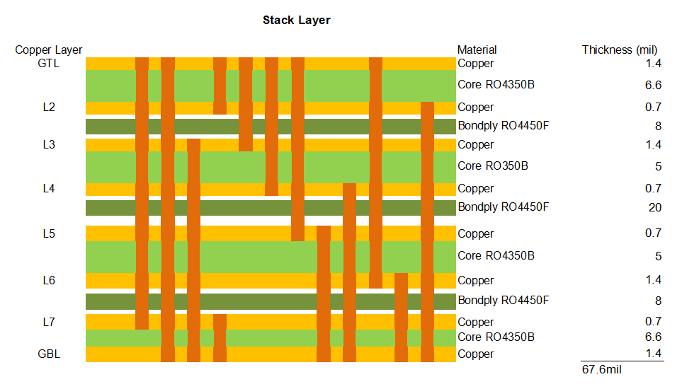
 - Base material: RO4350B

    - Layer count: 8 layers

    - Board dimensions:  96.4 mm x 163.9 mm=3Types =3PCS, +/- 0.15mm

    - Minimum Trace/Space:  4/6 mils

    - Minimum Hole Size:  0.4mm

    - Blind vias GTL-L7, L3-GBL, GTL-L2, L7-GBL, GTL-L3, GTL-L4, GTL-L5, L5-GBL, L4-GBL, GTL-L6, L6-GBL, L2-GBL, mechanical drill.

    - Finished board thickness:  1.8mm

    - Finished Cu weight:  1oz (1.4 mils)  outer layers;  1oz (1.4mil )/ 0.5oz (0.7mil) inner layers

    - Via plating thickness: 20 μm

    - Surface finish:  Electroless Nickel Immersion Gold

    - Top Silkscreen:          White

    - Bottom Silkscreen:      White

    - Top Solder Mask:  Green

    - Bottom Solder Mask: Green

    - All vias are resin filled and capped

    - 100% Electrical test used prior to shipment

    - Impedance controlled

     50 ohm on GTL 9.4mil, reference layer 2

     50 ohm on L2 7mil, reference layer GTL, L3/GND

     50 ohm on L7 7mil, reference layer L6/PWR, L8/GBL

     50 ohm on GBL 9.4mil, referance layer L7/GND


6. PCB Statistics:

    Components:        76

    Total Pads:         303

    Thru Hole Pads:     117

    Top SMT Pads:      121

    Bottom SMT Pads:    65

    Vias:              335

    Nets:              6

 
7. Type of artwork supplied: Gerber RS-274-X
 
8. Quality standard: IPC-Class-2
 
9. Availability: worldwide

10. Typical Applications:

- Cellular Base Station Antennas and Power Amplifiers

- RF Identification Tags

- Automotive Radar and Sensors

- LNB's for Direct Broadcast Satellites


NEXT: 6-Layer 370HR PCB 1.03mm ENIG High Temperature FR-4 with 180°C Tg for Demanding Multilayer Applications


About Us
Products
Solutions
Contact Us


Antenna, Mobile Internet
Address:
6-11C Shidai Jingyuan, Fuyong, Baoan, Shenzhen, Guangdong, China 518103


Wireless Infrastructure
Phone:
86-755-27374946


Millimeter Wave Radar
Email:
info@bicheng-enterprise.com


Aerospace
 
WeChat:
bichengpcb


Satellite Navigation
 
Teams:
vickyxie0315@outlook.com


Power Amplifier


IoT


in fb yt quora


Copyright  © Shenzhen Bicheng Electronics Technology Co., Ltd. All rights reserved