| |
|
|
|
|
|
|
|
|
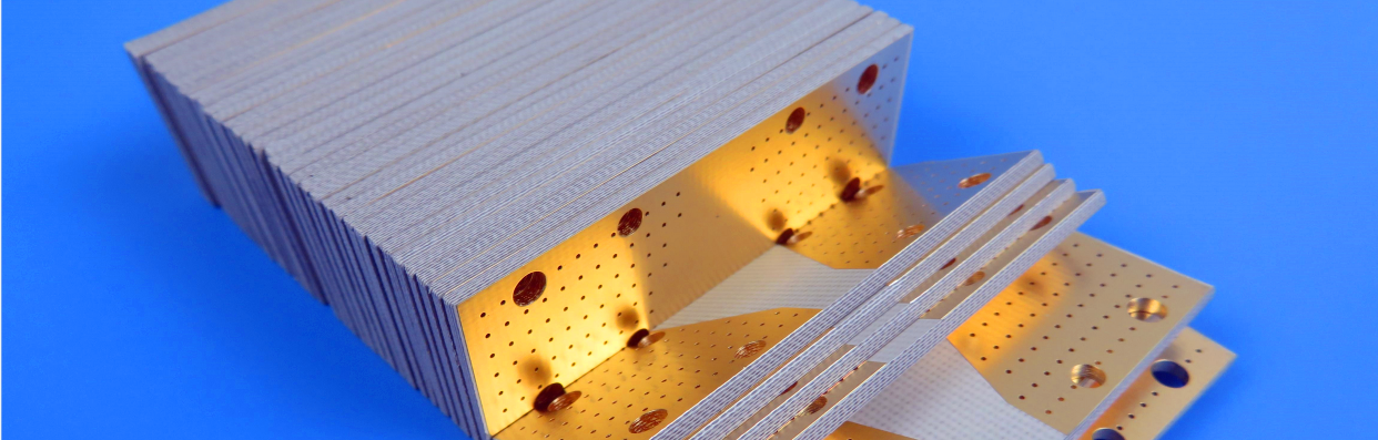
Impedance Controlled Flexible Printed Circuit on Polyimide 76 Micron Substrate with 90ohm Impedance for USB Connector |
|
|
(Flexible printed circuits are custom-made products. The picture and parameters shown are for reference only.) |
|
|
|
|
|
General description |
|
|
This flexible PCB features a 76-micron polyimide base substrate with precisely controlled 90-ohm impedance on 0.15mm/0.3mm trace/space configurations. The standard 0.20mm thick construction incorporates double-sided yellow solder mask coverlay and immersion gold surface finish on contact pads. FR-4 stiffeners are applied at both ends for enhanced structural support during connector mating cycles. Manufactured using Shengyi base materials, each production panel yields single-unit flex circuits. These IPC 6012 Class 2 compliant boards are produced from customer-supplied Gerber files and shipped in quantities of 25 pieces per package, ensuring consistent quality for connector interface applications. |
|
|
|
|
|
 |
|
|
|
|
|
Parameter and Data Sheet |
|
|
PCB Size: |
196 X 35mm = 1 PCS |
Number of Layers |
2 layers |
Board Type |
Flexbile PCB |
Board Thickness |
0.2mm +/-10% |
Stackup |
TOP FR-4 Steffener 0.8mm |
|
PI coverlay 0.025mm |
|
Copper top 0.035mm finish |
|
Polyimide substrate 0.076mm |
|
Copper top 0.035mm finish |
|
PI coverlay 0.025mm |
Board Material Supplier |
Shengyi |
Tg Value of Board Material |
60℃ |
|
PTH Cu thickness |
20 um |
Inner Iayer Cu thicknes |
N/A |
Surface Cu thickness |
35 um (1oz) |
|
Coverlay Colour |
Yellow |
Number of Coverlay |
2 |
Thickness of Coverlay |
25 um |
Stiffener |
FR-4 0.8mm |
|
Type of Silkscreen Ink |
N/A |
Supplier of Silkscreen |
N/A |
Color of Silkscreen |
N/A |
Number of Silkscreen |
N/A |
|
Minimum via (mm) |
0.3 |
Minimum Trace (mil) |
5.90 |
Minimum Gap(mil) |
11.8 |
|
Surface Finish |
Immersion Gold |
RoHS Required |
Yes |
Famability |
94-V0 |
|
Thermal Shock Test |
Pass, -25℃±125℃, 1000 cycles. |
Thermal Stress |
Pass, 300±5℃,10 seconds, 3 cycles. No delamination, no blistering. |
Function |
100% Pass electrical test |
Workmanship |
Compliance with IPC-A-600H & IPC-6013C Class 2 |
Type of artwork to be supplied |
email file, Gerber RS-274-X, PCBDOC etc |
Service area |
Worldwide, Globally. |
|
|
|
|
|
|
.jpg) |
|
|
|
|
|
Features and Benefits
1. Excellent flexibility
2. Reducing the volume
3. Weight reduction
4. Consistency of assembly
5. Increased reliability
6. Low cost
7. Continuity of processing
8. Robust PCB capabilities to support your R and D, sales, and marketing efforts
9. Reliable on-time delivery with an over 98% on-time delivery rate
10. Dedicated team embodying passion, discipline, responsibility, and integrity
11. No minimum order requirement – even a single piece is welcome |
|
|
|
|
|
Applications |
|
|
Flexible flat cable, Industrial control temperature controller soft board, medical equipment controller, automobile GPS navigation flex board, tablet keypad flex board, display backlight |
|
|
|
|
|
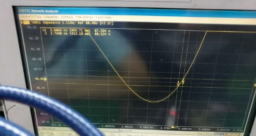
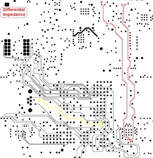
1.5 Single ended (line) impedance, Differential impedance Definition of Characteristic Impedance |
|
|
Definition of Characteristic Impedance
Characteristic impedance is defined as the total opposition presented to the propagation of high-frequency signals or electromagnetic waves along a transmission line with respect to a reference plane. This parameter is mathematically represented as the vector summation of the conductor's electrical resistance, inductive reactance, and capacitive reactance components at a specified operating frequency.
Classification of Characteristic Impedance
In printed circuit board design, characteristic impedance manifests in three fundamental configurations:
(1)Single-Ended Impedance: The characteristic impedance measured for an individual signal trace relative to its reference plane.
(2)Differential Impedance: The effective impedance exhibited between two parallel transmission lines of identical geometry when driven by complementary signals, accounting for both self-impedance and mutual coupling effects.
(3)Coplanar Impedance: The characteristic impedance measured when the signal line is transmitting between its surrounding GND / VCC (the space between the signal line to GND / VCC on both sides is equal).
These distinct impedance types each play critical roles in ensuring signal integrity across various high-speed circuit architectures, with proper impedance control being essential for minimizing reflections and maintaining signal quality in modern electronic systems. |
|
|
 |
|
|
|
|
|
The Determinant Condition Required for Impedance Control |
|
|
When signal propagation occurs along PCB conductors, the transmission line effect becomes significant when the conductor length approaches 1/7 of the signal wavelength. Under such conditions, the conductor transitions into a transmission line requiring controlled impedance characteristics. The implementation of impedance control in manufacturing is strictly customer-specified - when particular trace widths are designated for impedance matching, these parameters must be precisely maintained during production. The impedance matching system comprises three essential components: the output impedance (source component), the characteristic impedance (transmission line), and the input impedance (load component). This triad forms the critical foundation for maintaining signal integrity throughout the PCB circuit path. Proper coordination of these elements ensures optimal energy transfer and minimizes signal reflections across the entire transmission system. |
|
|
|
|
|
More Impedance Controlled Flexible Circuit (FPC) |
|
|
.jpg) |
|
|
|
|
|
.jpg) |
|
|
|
|
|
|
|
|
|
|
|
Hot Tags:
Flexible PCB Impedance Controlled |
Polyimide Flexible Circuit PCB |
Polyimide Flex PCB |
FPC PCB 90ohm Impedance Controlled |
Shengyi Flexible Circuit PCB |
|
|
|