|
|
|
|
Fabrication Guideline: DiClad 870
|
|
|
(This guideline is organized by BichengPCB based on authoritative publications by Rogers Corp. and you can also refer to the original text on the Rogers website)
|
|
|
|
|
|
MATERIAL DESCRIPTION |
|
|
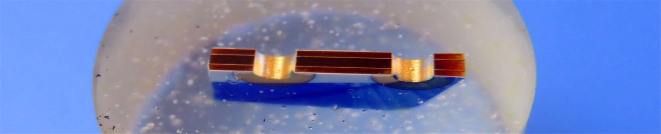
DiClad 870 laminates consist of woven fiberglass and PTFE composite materials, specifically designed as substrates for printed circuit boards. The woven fiberglass reinforcement in DiClad 870 offers enhanced dimensional stability compared to nonwoven fiberglass reinforced PTFE laminates that have similar dielectric constants. |
|
|
|
|
|
These guidelines aim to equip fabricators with fundamental information for processing double-sided and multi-layer boards using copper-clad DiClad 870 laminates. For more detailed processing guidance, it is advisable to contact a Rogers technical service engineer or sales representative. |
|
|
|
|
|
|
|
|
|
|
|
STORAGE |
|
|
DiClad 870 cores can be stored indefinitely under normal ambient conditions. Implementing a first-in-first-out (FIFO) inventory system is recommended, as it helps track material lot numbers throughout PCB processing and the delivery of finished circuits. |
|
|
|
|
|
Storage in Original Shipping Cartons |
|
|
Carton Placement: Place cartons on a flat surface, ensuring they are safely out of the way of mobile handling equipment. Cartons may be stored on their sides, provided that no heavy items are stacked on top. |
|
|
|
|
|
Stacking Limit: Do not stack cartons more than five high to prevent excessive weight on the lower packages. |
|
|
|
|
|
Storage of Panels Removed from Cartons |
|
|
|
|
|
1. Oxidation Considerations: DiClad 870 laminates with thick copper plates lack protective anti-tarnish layers, which means some discoloration due to oxidation may occur during storage, particularly in high temperature and humidity environments. This oxidation can be removed through mechanical (deburring) or chemical methods (microetch), both of which are standard in the PCB fabrication process. |
|
|
|
|
|
2. Storage of Thicker Panels: Panels thicker than 20 mils can be stored upright in slotted shelving units, ensuring that the clad surfaces remain vertical. This arrangement allows for easy access while minimizing the risk of damage to the metal surfaces. |
|
|
|
|
|
3.Alternative Storage Guidelines: If vertical stacking is not feasible: |
|
|
A) Ensure the shelf is flat, smooth, and clean. |
|
|
B) The shelf should extend beyond the full area of the panels being stored. |
|
|
C) Ensure that the surfaces of the laminates are clear of debris. |
|
|
D) Keep shelf loading below 50 pounds per square foot. |
|
|
E) Interleave panels with soft, non-abrasive separator sheets. |
|
|
|
|
|
Handling |
|
|
PTFE-based materials are softer than most other rigid printed circuit board laminates, making them more vulnerable to handling damage. Cores that are clad solely with copper foils can easily become creased, while materials bonded to thick aluminum, brass, or copper plates are more susceptible to scratches, pits, and dents. It is essential to adhere to proper handling procedures. |
|
|
|
|
|
1. Glove Use: Always wear gloves made of knit nylon or other non-absorbent materials when handling panels. Natural skin oils are slightly acidic and can corrode copper surfaces. Fingerprints are particularly challenging to remove, as standard brighteners may dissolve corrosion but leave behind oils that can cause fingerprints to reappear after hours or days. To effectively remove fingerprints, follow this procedure: |
|
|
A) Bright dip in a dilute hydrochloric acid solution. |
|
|
B) Degrease using acetone, methyl ethyl ketone, or by vapor degreasing with chlorinated solvents. |
|
|
C) Rinse with water and bake dry for 60 minutes at 250°F (125°C). |
|
|
D) Repeat the bright dip. |
|
|
|
|
|
2. Work Surface Maintenance:?Ensure that work surfaces are clean, dry, and free from debris. |
|
|
3. Keep Protective Covers:?Retain the polyethylene bag or sheet during initial processes such as shearing, sawing, blanking, and punching. |
|
|
4. Proper Lifting Technique:?Always lift panels by two edges. Thin cores, in particular, lack the necessary stiffness to be supported by a single edge or corner, which could lead to dimensional distortion or permanent creasing. |
|
|
5. Transporting Cores: During processing, transport cores between workstations on flat carrying trays, ideally interleaved with soft, sulfur-free paper. Avoid using vertical racks unless they are slotted and provide sufficient vertical support. |
|
|
|
|
|
INNER LAYER PREPARATION |
|
|
|
|
|
Tooling |
|
|
DiClad 870 materials are compatible with a variety of tooling systems. The choice between round or slotted pins, external or internal pinning, standard or multiline tooling, and whether to use pre- or post-etch punching depends on the circuit facility's capabilities and the final registration requirements. |
|
|
|
|
|
Generally, slotted pins, a multiline tooling format, and post-etch punching will fulfill most requirements. Regardless of the method chosen, it is advisable to retain copper around tooling holes. |
|
|
|
|
|
A flow pattern that aligns with the selected adhesive system can be utilized between circuits and around the panel's perimeter. However, retaining as much copper as possible typically enhances layer registration. |
|
|
|
|
|
Surface Preparation for Photoresist Application |
|
|
The preferred method for preparing copper surfaces for liquid or film photoresist application is a chemical process that includes organic cleaners followed by a microetch. A conveyorized spray system with an abrasive substance suspended in solution can also be used, though it carries a slight risk to registration control. Mechanical scrubbing should only be considered for thicker cores (0.060§+) and should be performed at reduced pressures to avoid distorting the thin laminate or creating deep scratches that could affect the spacing between copper planes. |
|
|
|
|
|
Photoresist Application |
|
|
Liquid or dry film photoresist can be applied using traditional techniques such as dip or spray coating, screening, or roll lamination. |
|
|
|
|
|
DES Processing |
|
|
Developers, strippers, and copper etchants suitable for processing epoxy glass materials will also be effective with DiClad 870?layers. Thin cores may need leader boards for conveyorized processing and frames or supportive racks for vertical processing methods. The ceramic-filled material will necessitate more stringent rinse and bake procedures, depending on the subsequent steps in the process sequence. |
|
|
|
|
|
Oxide Treatment |
|
|
DiClad 870 cores are compatible with most oxide processes and alternative oxide treatments. It is advisable to follow the process recommended by the adhesive system supplier chosen for bonding the multilayer board. For highly caustic, high-temperature processes, such as traditional or reduced black oxides, ensure a thorough rinse and bake of the inner layers afterward. |
|
|
|
|
|
BONDING |
|
|
|
|
|
Bonding Preparation |
|
|
While special pretreatments of etched surfaces using sodium or plasma processes are acceptable, they are generally unnecessary if care has been taken to protect the substrate surface after copper etching. Inner layers should be baked at 110°C to 125°C (230°F to 260°F) for 30 to 120 minutes to eliminate volatile substances before multilayer board bonding. Refer to the guidelines for oxide treatment to ensure that the dry bake does not degrade the bond-enhancing surface. |
|
|
|
|
|
Multilayer Adhesive System |
|
|
DiClad 870?cores are compatible with a wide variety of thermosetting adhesives (such as FR-4, Rogers' 2929 bondply, RO4400 prepreg) and thermoplastic adhesives (including 3001 Bonding Film, CuClad 6250 & 6700 Bonding Films, CLTE-P, FEP, PFA, and PTFE). When selecting the most suitable adhesive system, factors such as electrical performance, flow characteristics, ease of processing, and bond temperature requirements should be taken into account. Rogers' Technical Service Engineers (TSEs) are knowledgeable about these trade-offs and can assist with the selection process upon request. |
|
|
|
|
|
Multilayer Bond Cycle |
|
|
The press cycle duration is dictated by the specifications of the chosen adhesive system. When using thermoplastic (meltable) films, cooling under pressure is necessary. |
|
|
|
|
|
PTH & OUTER LAYER/DOUBLE-SIDED CIRCUIT PROCESSING |
|
|
|
|
|
Drilling |
|
|
Double-sided boards can be drilled either as individual pieces or in stack heights compatible with the flute length of the drills used. Multilayers are typically drilled in single stacks. For entry layers (0.010" to 0.030" thick), phenolic composite boards are recommended, while exit layers (greater than 0.060§) can also use sheeted aluminum and metal-coated phenolic boards. |
|
|
|
|
|
New carbide drills are highly recommended, and both standard and undercut styles can be utilized. Recommended chip loads range from 0.001" to 0.003" per revolution, with surface speeds between 150 and 300 SFM, varying with tool diameter〞slower feeds and speeds are preferable for finer diameter drills. The retract rate for drilling double-sided and multilayer boards should be between 300 and 500 IPM, and 700 to 1000 IPM for double-sided constructions. |
|
|
|
|
|
Tool life should be assessed through the inspection of cross-sectioned holes, especially when drilling multilayer boards, as factors like adhesive type, inner-layer copper weight, and board thickness influence hole quality and tool longevity. The "twelve inch rule," which suggests replacing a tool after drilling 12 inches of substrate, is a useful guideline for establishing tool life for multilayer constructions. For example, when drilling a 0.060§ thick board, the initial hit count would be 12§ divided by 0.060§ = 200 holes. |
|
|
|
|
|
Deburring |
|
|
To minimize the risk of copper burring, use flat, rigid entry materials, conservative drilling parameters, and limit hit counts with new drills. When drilled correctly, cores should be prepared for subsequent processing. If deburring is necessary and minimal, a chemical microetch process is preferred. If mechanical processing is required, a hand pumice scrub is recommended over a suspended abrasive spray system, which should be preferred over a conveyorized mechanical deburr or planarization process. |
|
|
|
|
|
Hole Preparation |
|
|
Loosely deposited debris within the holes can be removed using a vapor or hydro-honing process, which directs water-suspended abrasive particles through the drilled holes. It is crucial to properly support the soft laminates during these processes. |
|
|
|
|
|
PTFE composites generally do not require desmearing. However, the adhesive system used to bond multilayer boards may necessitate a desmear process, which can be achieved using either a chemical (permanganate) or plasma (CF4/O2) method. Neither process significantly affects the PTFE materials but should be conducted prior to activating the PTFE surface. If plasma is chosen for desmearing, a dual cycle can be implemented to desmear the adhesive system and activate the PTFE surface. This involves adding the desmear cycle outlined below to the beginning of the treatment cycle described in this section. Additionally, DiClad 870 materials may require a glass etch to reduce the risk of plated nodules. |
|
|
|
|
|
Drilled holes in PTFE-based laminates must be treated before applying a conductive seed layer (e.g., electroless copper or direct metallization). Failing to perform a surface activation treatment can lead to poor metal adhesion or plated voids. Common pre-treatments for PTFE materials include sodium treatment and plasma treatment, with sodium treatment being preferred, though either can be used for DiClad 870?materials. |
|
|
|
|
|
Panels should be baked for a minimum of 1 hour at 110 to 125°C (230 to 260°F) prior to plasma treatment. Note that plasma-treated holes are more delicate than sodium-etched holes, and panels should not undergo any pressure washing or scrubbing processes before metallization. |
|
|
|
|
|
Metallization |
|
|
DiClad 870 materials are compatible with conventional electroless copper and direct deposit metallization processes. Before metal deposition, cores should be baked for 30 to 90 minutes at 110°C to 125°C (230°F to 260°F), unless plasma treatment has been used, which also serves as a vacuum bake to prepare the hole walls for plating. A flash plate build-up of 0.0001§ to 0.0003§ (0.0025mm to 0.0076mm) of copper is recommended to enhance support for the hole walls in preparation for outer-layer processing. |
|
|
|
|
|
PTH Plating & Outer-Layer Imaging |
|
|
Standard equipment and chemical processes are utilized to plate, image, and etch circuit patterns onto DiClad materials. It is important to take care in preserving the laminate surface after etching, as the resulting topography enhances adhesion to solder masks. |
|
|
|
|
|
Final Surfaces |
|
|
Materials should be rinsed and baked before applying solder mask. A rinse in warm or hot water for 20 to 30 minutes, followed by a 60-minute bake at 125°C (260°F), is generally adequate, especially if the bake occurs under vacuum. Properly prepared DiClad 870?materials are compatible with most liquid photoimageable (LPI) solder masks, with epoxy masks preferred for applications requiring selective silk screening. |
|
|
|
|
|
Most final finishes (such as HASL, Sn, Ag, Ni/Au, OSP, etc.) have been successfully applied to DiClad 870?materials without any issues or special considerations. If a rinse/bake regimen has not been performed as part of the solder mask application, it should be completed prior to HASL or reflow exposures. When using flux, acid fluxes are recommended over solvent-based ones. The HASL or reflow exposure should occur as soon as possible after the flux application. |
|
|
|
|
|
Final Circuitization |
|
|
Individual circuits can be routed, punched, or lasered according to preference, tolerances, and edge quality requirements. It is advisable to pre-route vacuum channels in the backer board to ensure proper airflow during routing. For the cleanest edge quality, double-pass routing in opposite directions is recommended. |
|
|
|
|