| |
|
|
|
|
|
|
|
|
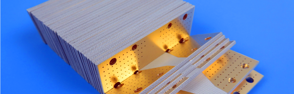
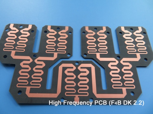
DK2.2 Dual Layer F4BME220 High Frequency PCB PTFE Cheap RF PWB for Couplers |
|
|
(Printed Circuit Boards are custom-made products. The picture and parameters shown are for reference only.) |
|
|
|
|
|
Brief Introduction
This PCB measures 100 x 100 mm and is designed as a double-sided, two-layer board. It accommodates surface mount components only, excluding through-hole components. The layer stackup features a top layer of 35 µm (1 oz) copper with an initial plating of 0.5 oz, paired with a 1.0 mm thick F4BME220 core material, and a matching bottom layer of 35 µm (1 oz) copper. The surface finish is Organic Solderability Preservative (OSP), ensuring reliable soldering performance. Notably, this PCB does not include a solder mask. |
|
|
|
|
|
The details are presented in the table below. |
|
|
|
|
|
PCB Specifications |
|
|
|
|
|
F4BME220 High Frequency PCB On DK2.2 Dual Layer Cheap RF PTFE PWB for Couplers |
|
|
PCB SIZE |
100 x 100mm=1PCS |
BOARD TYPE |
Double sided PCB |
Number of Layers |
2 layers |
Surface Mount Components |
YES |
Through Hole Components |
NO |
LAYER STACKUP |
copper ------- 35um(0.5 oz +plate) TOP layer |
F4BME220 1.0mm |
copper ------- 35um(0.5 oz + plate) BOT Layer |
TECHNOLOGY |
|
Minimum Trace and Space: |
10 mil / 10 mil |
Minimum / Maximum Holes: |
0.4 mm / 0.4 mm |
Number of Different Holes: |
1 |
Number of Drill Holes: |
1 |
Number of Milled Slots: |
0 |
Number of Internal Cutouts: |
0 |
Impedance Control: |
no |
Number of Gold finger: |
0 |
BOARD MATERIAL |
|
Glass Epoxy: |
F4BME220 DK 2.2 |
Final foil external: |
1oz |
Final foil internal: |
N/A |
Final height of PCB: |
1.1 mm ±10% |
PLATING AND COATING |
|
Surface Finish |
OSP |
Solder Mask Apply To: |
no |
Solder Mask Color: |
no |
Solder Mask Type: |
no |
CONTOUR/CUTTING |
Routing |
MARKING |
|
Side of Component Legend |
NO |
Colour of Component Legend |
NO |
Manufacturer Name or Logo: |
Marked on the board in a conductor and leged FREE AREA |
VIA |
Non-Plated through hole(PTH), minimum size 0.4mm. |
FLAMIBILITY RATING |
UL 94-V0 Approval MIN. |
DIMENSION TOLERANCE |
|
Outline dimension: |
0.0059" |
Board plating: |
0.0029" |
Drill tolerance: |
0.002" |
TEST |
100% Electrical Test prior shipment |
TYPE OF ARTWORK TO BE SUPPLIED |
email file, Gerber RS-274-X, PCBDOC etc |
SERVICE AREA |
Worldwide, Globally. |
|
|
 |
|
F4BME High Frequency Laminates
F4BME series laminates are engineered through a precise formulation and rigorous pressing of fiberglass cloth, polytetrafluoroethylene resin, and polytetrafluoroethylene film. These laminates offer enhanced electrical performance compared to F4B, featuring a broader range of dielectric constants, reduced dielectric loss, increased insulation resistance, and improved stability. They serve as suitable replacements for similar foreign products. |
|
|
|
|
|
Features
◆ DK2.17 ~ 3.0 is optional, and DK can be customized
◆ Low loss
◆ F4BME with RTF copper foil has excellent PIM index
◆ Diversified size and cost saving
◆ Irradiation resistance and low exhaust
◆ Commercialization, mass production and high cost performance |
|
|
|
|
|
Typical Applications
◆ Microwave, RF, radar
◆ Phase shifter, passive components
◆ Power divider, coupler and combiner
◆ Feed network, phased array antenna
◆ Satellite communication, base station antenna |
|
|
|
|
|
Our PCB Capability(F4BME) |
|
|
PCB Capability (F4BME) |
PCB Material: |
PTFE glass fiber cloth copper clad laminates |
Designation (F4BME ) |
F4BME |
DK (10GHz) |
DF (10 GHz) |
|
F4BME217 |
2.17±0.04 |
0.0010 |
|
F4BME220 |
2.20±0.04 |
0.0010 |
|
F4BME233 |
2.33±0.04 |
0.0011 |
|
F4BME245 |
2.45±0.05 |
0.0012 |
|
F4BME255 |
2.55±0.05 |
0.0013 |
|
F4BME265 |
2.65±0.05 |
0.0013 |
|
F4BME275 |
2.75±0.05 |
0.0015 |
|
F4BME294 |
2.94±0.06 |
0.0016 |
|
F4BME300 |
3.00±0.06 |
0.0017 |
Layer count: |
Single Sided, Double Sided PCB, Multilayer PCB, Hybrid PCB |
Copper weight: |
0.5oz (17 µm), 1oz (35µm), 2oz (70µm) |
Dielectric thickness (or overall thickness) |
0.127mm (dielectric), 0.2mm, 0.25mm, 0.5mm, 0.508mm, 0.762mm, 0.8mm, 1.0mm, 1.5mm, 1.524mm, 1.575mm, 2.0mm, 2.5mm, 3.0mm, 4.0mm, 5.0mm, 6.0mm, 8.0mm, 10.0mm, 12.0mm |
PCB size: |
≤400mm X 500mm |
Solder mask: |
Green, Black, Blue, Yellow, Red etc. |
Surface finish: |
Bare copper, HASL, ENIG, Immersion silver, Immersion tin, OSP, Pure gold, ENEPIG etc.. |
|
|
|
Data Sheets (F4BME) |
|
|
Product Technical Parameters |
Product Model & Data Sheet |
Product Features |
Test Conditions |
Unit |
F4BME
217 |
F4BME
220 |
F4BME
233 |
F4BME
45 |
F4BME
255 |
F4BME
265 |
F4BME
275 |
F4BME
294 |
F4BME
300 |
Dielectric Constant (Typical) |
10GHz |
/ |
2.17 |
2.2 |
2.33 |
2.45 |
2.55 |
2.65 |
2.75 |
2.94 |
3.0 |
Dielectric Constant Tolerance |
/ |
/ |
±0.04 |
±0.04 |
±0.04 |
±0.05 |
±0.05 |
±0.05 |
±0.05 |
±0.06 |
±0.06 |
Loss Tangent (Typical) |
10GHz |
/ |
0.001 |
0.001 |
0.0011 |
0.0012 |
0.0013 |
0.0013 |
0.0015 |
0.0016 |
0.0017 |
|
20GHz |
/ |
0.0014 |
0.0014 |
0.0015 |
0.0017 |
0.0018 |
0.0019 |
0.0021 |
0.0023 |
0.0025 |
Dielectric Constant Temperature Coefficient |
-55ºC~150ºC |
PPM/℃ |
-150 |
-142 |
-130 |
-120 |
-110 |
-100 |
-92 |
-85 |
-80 |
Peel Strength |
1 OZ F4BM |
N/mm |
>1.8 |
>1.8 |
>1.8 |
>1.8 |
>1.8 |
>1.8 |
>1.8 |
>1.8 |
>1.8 |
|
1 OZ F4BME |
N/mm |
>1.6 |
>1.6 |
>1.6 |
>1.6 |
>1.6 |
>1.6 |
>1.6 |
>1.6 |
>1.6 |
Volume Resistivity |
Standard Condition |
MΩ.cm |
≥6×10^6 |
≥6×10^6 |
≥6×10^6 |
≥6×10^6 |
≥6×10^6 |
≥6×10^6 |
≥6×10^6 |
≥6×10^6 |
≥6×10^6 |
Surface Resistivity |
Standard Condition |
MΩ |
≥1×10^6 |
≥1×10^6 |
≥1×10^6 |
≥1×10^6 |
≥1×10^6 |
≥1×10^6 |
≥1×10^6 |
≥1×10^6 |
≥1×10^6 |
Electrical Strength (Z direction) |
5KW,500V/s |
KV/mm |
>23 |
>23 |
>23 |
>25 |
>25 |
>25 |
>28 |
>30 |
>30 |
Breakdown Voltage (XY direction) |
5KW,500V/s |
KV |
>30 |
>30 |
>32 |
>32 |
>34 |
>34 |
>35 |
>36 |
>36 |
Coefficientof Thermal Expansion |
XY direction |
-55 º~288ºC |
ppm/ºC |
25, 34 |
25, 34 |
22, 30 |
20, 25 |
16, 21 |
14, 17 |
14, 16 |
12, 15 |
12, 15 |
|
Z direction |
-55 º~288ºC |
ppm/ºC |
240 |
240 |
205 |
187 |
173 |
142 |
112 |
98 |
95 |
Thermal Stress |
260℃, 10s,3 times |
No delamination
|
Water Absorption |
20±2℃, 24 hours |
% |
≤0.08 |
≤0.08 |
≤0.08 |
≤0.08 |
≤0.08 |
≤0.08 |
≤0.08 |
≤0.08 |
≤0.08 |
Density |
Room Temperature |
g/cm3 |
2.17 |
2.18 |
2.20 |
2.22 |
2.25 |
2.25 |
2.28 |
2.29 |
2.29 |
Long-Term Operating Temperature |
High-Low Temperature Chamber |
℃ |
-55~+260 |
-55~+260 |
-55~+260 |
-55~+260 |
-55~+260 |
-55~+260 |
-55~+260 |
-55~+260 |
-55~+260 |
Thermal Conductivity |
Z direction |
W/(M.K) |
0.24 |
0.24 |
0.28 |
0.30 |
0.33 |
0.36 |
0.38 |
0.41 |
0.42 |
PIM |
Only applicable to F4BME |
dBc |
≤-159 |
≤-159 |
≤-159 |
≤-159 |
≤-159 |
≤-159 |
≤-159 |
≤-159 |
≤-159 |
Flammability |
/ |
UL-94 |
V-0 |
V-0 |
V-0 |
V-0 |
V-0 |
V-0 |
V-0 |
V-0 |
V-0 |
Material Composition |
/ |
/ |
PTFE, Fiberglass Cloth
F4BM paired with ED copper foil, F4BME paired with reverse-treated (RTF) copper foil. |
|
|
|
|
|
|
|
|
|
|
|
|
Hot Tags:
| Dual Layer F4BME220 PCB |
DK 2.2 Wangling Substrate |
F4BME220 High Frequency PCB |
F4BME220 PCB Datasheet |
Low Dielectric Loss PCB |
|
|
|