|
|
|
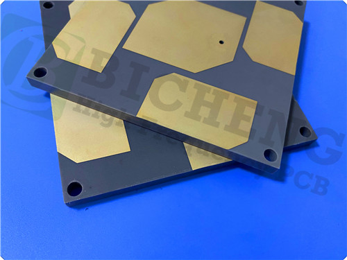
Customized Double Sided Wangling 5.08mm F4BTMS615 Material PCB HASL Surface Finish |
|
|
|
|
|
|
|
1. F4BTMS Introduction
The F4BTMS series represents an advanced iteration of the F4BTM series, boasting a significant technological advancement in both material composition and manufacturing techniques. Enriched with a substantial amount of ceramics and reinforced with ultra-thin, ultra-fine glass fiber cloth, this material exhibits substantial improvements in performance and offers a wider range of dielectric constants. It is highly reliable and ideal for aerospace applications, serving as a viable replacement for comparable foreign products.
|
|
|
|
By integrating a small quantity of ultra-thin, ultra-fine glass fiber cloth with a substantial, uniformly dispersed mixture of special nano-ceramics and polytetrafluoroethylene resin, the material minimizes the adverse effects of glass fiber on electromagnetic wave propagation. This results in reduced dielectric loss, enhanced dimensional stability, and decreased anisotropy across the X/Y/Z axes. Furthermore, it expands the usable frequency range, bolsters electrical strength, and enhances thermal conductivity. The material also demonstrates an exceptional low thermal expansion coefficient and stable dielectric temperature characteristics. |
|
|
|
As a standard feature, the F4BTMS series includes RTF low roughness copper foil, which minimizes conductor loss and offers robust peel strength. It is compatible with both copper and aluminum bases. |
|
|
|
2. Features of F4BTMS615:
Dielectric Constant (Dk): 6.15 at 10GHz
Dissipation Factor: 0.0020 at 10GHz, 0.0023 at 20GHz
Coefficient of Thermal Expansion (CTE):
X-axis: 10 ppm/°C
Y-axis: 12 ppm/°C
Z-axis: 40 ppm/°C (within the temperature range of -55°C to 288°C)
Low Thermal Coefficient of Dk: -96 ppm/°C (within the temperature range of -55°C to 150°C)
High Thermal Conductivity: 0.67 W/mk
Moisture Absorption: 0.1%
|
|
|
|
3. PCB Stackup: 2-layer rigid PCB
Copper_layer_1 - 35 μm
F4BTMS615 Core - 5.08 mm (200mil)
Copper_layer_2 - 35 μm |
|
|
|
| 4. PCB Construction Details: |
| |
| - Board dimensions: 92.32mm x 31.5 mm=1PCS, +/- 0.15mm
- Minimum Trace/Space: 5/5 mils
- Minimum Hole Size: 0.5mm
- No Blind vias.
- Finished board thickness: 5.2mm
- Finished Cu weight: 1oz (1.4 mils) outer layers
- Via plating thickness: 20 μm
- Surface finish: Hot Air Soldering Level (HASL)
- Top Silkscreen: No
- Bottom Silkscreen: No
- Top Solder Mask: No
- Bottom Solder Mask: No
- 100% Electrical test used prior to shipment |
| |
|
 |
|
|
|
|
5. PCB Statistics:
Components: 20
Total Pads: 35
Thru Hole Pads: 21
Top SMT Pads: 14
Bottom SMT Pads: 0
Vias: 37
Nets: 2
|
|
|
|
6. Type of artwork supplied: Gerber RS-274-X |
|
|
|
7. Quality standard: IPC-Class-2 |
|
|
|
8. Availability: worldwide |
|
|
|
9. Some Typical Applications:
- Aerospace equipment, including space and cabin systems.
- Microwave and RF technologies.
- Military and commercial radar systems.
- Feed networks for various applications.
- Phase-sensitive and phased array antennas.
- Satellite communications, and numerous other applications. |
|
|
|
|
|
|
|
|
|
|
|
|
|
NEXT:High Tg 175⊥ 4-layer 1.6mm IT-180ATC Rigid PCB with Lead Free Assembly Process |
|
|
|
|
|
|