|
|
|
2-layer-250mil-6.35mm-Thick-Wangling-F4BTMS220-High-Frequency-PCB-with-Low-DF-0.0010-for-Aerospace |
|
|
|
|
|
|
|
1. F4BTMS Introduction
The F4BTMS series represents a groundbreaking upgrade to the F4BTM series, achieving significant advancements in material formulation and manufacturing processes. Enriched with a high ceramic content and reinforced with ultra-thin, ultra-fine glass fiber cloth, this material delivers superior performance and a wider range of dielectric constants. Designed for high-reliability applications, the F4BTMS series is an ideal choice for aerospace and can seamlessly replace similar foreign products.
|
|
|
|
By integrating a unique blend of ultra-thin glass fiber cloth and specially formulated nano-ceramics with polytetrafluoroethylene resin, the F4BTMS series minimizes the negative impact of glass fibers on electromagnetic wave propagation. This innovative composition reduces dielectric loss, enhances dimensional stability, and decreases X/Y/Z anisotropy. The result is a material with an extended usable frequency range, improved electrical strength, and superior thermal conductivity. Additionally, the F4BTMS series boasts a low thermal expansion coefficient and stable dielectric temperature characteristics, ensuring consistent performance in demanding environments. |
|
|
|
The F4BTMS series comes standard with RTF low roughness copper foil, which reduces conductor loss and provides excellent peel strength. Compatible with both copper and aluminum bases, this material is a versatile and reliable solution for high-frequency applications. Whether for aerospace, telecommunications, or advanced electronics, the F4BTMS series sets a new standard for performance and durability. |
|
|
|
2. Features of F4BTMS220:
- Dielectric constant (Dk) of 2.2 at 10GHz
- Dissipation factor of .0009 at 10GHz, 0.0010 at 20GHz
- CTE x-axis of 40 ppm/°C, CTE y-axis of 50 ppm/°C, CTE z-axis of 290 ppm/°C, -55°C to 288°C
- Low thermal coefficient of Dk at-130 ppm/°C, -55°C to 150°C
- UL-94 V0
- Low Moisture absorption of 0.02%
|
|
|
|
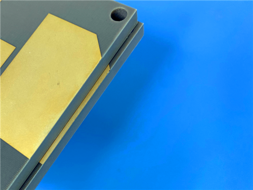
3. PCB Stackup: 2-layer rigid PCB
Copper_layer_1 - 35 μm
F4BTMS220 Core - 6.35 mm (250mil)
Copper_layer_2 - 35 μm |
|
| 4. PCB Construction Details: |
| |
| - Board dimensions: 75mm x 75mm=1PCS, +/- 0.15mm
- Minimum Trace/Space: 5/9 mils
- Minimum Hole Size: 0.6mm
- No Blind vias.
- Finished board thickness: 6.4mm
- Finished Cu weight: 1oz (1.4 mils) outer layers
- Via plating thickness: 20 μm
- Surface finish: Pure gold
- Top Silkscreen: No
- Bottom Silkscreen: No
- Top Solder Mask: No
- Bottom Solder Mask: No
- 100% Electrical test used prior to shipment |
| |
|
 |
|
|
5. PCB Statistics:
Components: 8
Total Pads: 20
Thru Hole Pads: 12
Top SMT Pads: 8
Bottom SMT Pads: 0
Vias: 23
Nets: 2
|
|
|
|
6. Type of artwork supplied: Gerber RS-274-X |
|
|
|
7. Quality standard: IPC-Class-2 |
|
|
|
8. Availability: worldwide |
|
|
|
9. Some Typical Applications:
- Aerospace equipment, including space and cabin systems.
- Microwave and RF technologies.
- Military and commercial radar systems.
- Feed networks for various applications.
- Phase-sensitive and phased array antennas.
- Satellite communications. |
|
|
|
|
|
|
|
|
|
|
|
|
|
NEXT: 12.9mm-Thick-Wangling-F4BTMS1000-PCB: 4-Layer-Aerospace-Material-with-Enhanced Dielectric-Properties-and-Superior-Thermal-Conductivity |
|
|
|
|
|
|
