|

|
|
|
|
16-Layer 2.0mm M6 PCB Optimized for 5G HPC and High Speed Servers with Low Dielectric Loss 0.002 |
|
|
|
|
|
|
|
1. Introduction of High Speed, Low Loss Multi-layer Materials -Megtron6 (M6) R-5775
Panasonic’s Megtron6 (M6) R-5775 is a cutting-edge multilayer copper-clad laminate (CCL) engineered for high-frequency, high-speed, and ultra-reliable electronic applications. Designed to excel in demanding environments, M6 is the material of choice for 5G communications, millimeter-wave radar, high-speed servers, and high-performance computing (HPC). With its industry-leading low dielectric loss (Df), stable dielectric constant (Dk), and exceptional thermal reliability, M6 ensures superior signal integrity and performance, even in the most challenging high-frequency transmission scenarios. Elevate your designs with M6 – the ultimate solution for next-generation electronics.
|
|
|
|
2. Features
- Dielectric Constant of DK 3.4 at 1GHz/23°C, 3.34 at 13GHz
- Dissipation Factor of 0.002 at 1GHz/23°C, 0.0037 at 13GHz
- X axis CTE of 16 ppm/°C, Y CTE of 16 ppm/°C, Z CTE of 45 ppm/°C
- High Tg value of >185 °C, DSC method, 210°C DMA method.
- Thermal Decomposition Temp ( Td ), 410°C, TGA method.
- Supports 4 - 30 layer multilayer PCB design, adapting to complex circuit requirements
- Complies with RoHS and halogen - free requirements, meeting the standards of green manufacturing.
- Compatible with traditional FR-4 processing technology, no special equipment is required, reducing production costs.
- Flammability of UL 94V-0 |
|
|
|
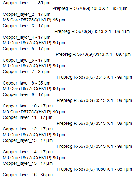
3. PCB Stackup: 16-layer rigid PCB
|
|
| 5. PCB Construction Details: |
| |
| - Board dimensions: 110 mm x 110 mm=1PCS, +/- 0.15mm
- Minimum Trace/Space: 3/4 mils
- Minimum Hole Size: 0.2mm
- No Blind vias.
- Finished board thickness: 2.0mm
- Finished Cu weight: 1oz (1.4 mils) outer layers, 0.5oz /1oz inner layers
- Via plating thickness: 25 μm
- Surface finish: Electroless Nickle Immersion Gold (ENIG)
- Top Silkscreen: White
- Bottom Silkscreen: White
- Top Solder Mask: Green
- Bottom Solder Mask: Green
- 0.2mm via filled and capped
- 100% Electrical test used prior to shipment |
| |
|
 |
|
|
5. Impedance controll:
Single-end, L1 11.8mil, 75ohm, reference layer 4
Single-end, L1, 5.9mil, 50 ohm, reference layer 2
Single-end, L16, 5.9mil, 50 ohm, reference layer 15
Differential, L1, 5.9mil/7.87mil, 100 ohm, reference layer 2
Differential, L10, 3.94mil/5.9mil, 100 ohm, reference layer 9
Differential, L12, 3.94mil/5.9mil, 100 ohm, reference layer 11, layer 13 |
|
|
|
6. PCB Statistics:
Components: 154
Total Pads: 406
Thru Hole Pads: 137
Top SMT Pads: 121
Bottom SMT Pads: 148
Vias: 532
Nets: 9
|
|
|
|
7. Type of artwork supplied: Gerber RS-274-X |
|
|
|
8. Quality standard: IPC-Class-2 |
|
|
|
9. Availability: worldwide |
|
|
|
10. Some Typical Applications:
- 5G Communication Base Stations: Millimeter-wave antennas, radio - frequency front - ends of AAU (Active Antenna Unit).
- Automotive Electronics: 77GHz millimeter-wave radar, ADAS (Advanced Driver - Assistance Systems).
- Data Centers: High-speed server motherboards, 400G/800G optical module PCBs.
- Aerospace: High-frequency circuit boards for satellite communication and radar systems.
- Consumer Electronics: High-frequency Wi-Fi 6E/7 routers, AR/VR devices.
|
|
|
|
|
|
|
|
|
|
|
|
|
|
NEXT: SF305 PCB 0.24mm Thick 25um Polyimide 2-Layer FPC Halogen-Free Flame Resistant for High Flex Applications by Shengyi |
|
|
|
|
|
|
|
|