| |
|
|
|
|
|
|
|
|
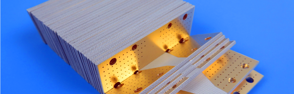
0.6mm F4BM300 High-Frequency PCB PTFE Substrate 2oz Copper Immersion Gold Precision for Radar and Satellite Communication |
|
|
(Printed Circuit Boards are custom-made products. The picture and parameters shown are for reference only.) |
|
|
|
|
|
Brief Introduction |
|
|
F4BM300 PCB adopts a square configuration measuring 85mm x 85mm, featuring a double-sided design with two copper layers. It is optimized for surface mount technology (SMT) components, and through-hole components are not supported in this layout.
The layer stackup includes a top layer constructed with 70 µm (2 oz) copper, starting with a 1 oz base plating, paired with a robust F4BM300 core material that is 0.508 mm thick. The bottom layer is also built with 70 µm (1 oz) copper, including plating, to ensure consistent and reliable performance.
The surface finish employs Immersion Gold, which improves solderability and offers superior corrosion resistance. A black solder mask is applied to the top side, providing both a durable protective layer and an aesthetically pleasing finish while shielding the internal circuitry.
Below is a detailed table summarizing the specifications: |
|
|
F4BM300 High Frequency PCB 0.6mm PTFE substrates 2oz Copper With Immersion Gold |
|
|
PCB SIZE |
85 x 85mm=1PCS |
BOARD TYPE |
Double sided PCB |
Number of Layers |
2 layers |
Surface Mount Components |
YES |
Through Hole Components |
NO |
LAYER STACKUP |
copper ------- 70um (1 oz+plate) TOP layer |
|
F4BM300 - 0.508mm |
|
copper ------- 70um(1 oz + plate) BOT Layer |
TECHNOLOGY |
|
Minimum Trace and Space: |
5 mil / 8 mil |
Minimum / Maximum Holes: |
0.3 mm / 1.2 mm |
Number of Different Holes: |
5 |
Number of Drill Holes: |
79 |
Number of Milled Slots: |
2 |
Number of Internal Cutouts: |
2 |
Impedance Control: |
no |
Number of Gold finger: |
0 |
BOARD MATERIAL |
|
Glass Epoxy: |
F4BM300 DK 3.0 |
Final foil external: |
2oz |
Final foil internal: |
N/A |
Final height of PCB: |
0.6 mm ±10% |
PLATING AND COATING |
|
Surface Finish |
Immersion gold |
Solder Mask Apply To: |
Top |
Solder Mask Color: |
Black |
Solder Mask Type: |
no |
CONTOUR/CUTTING |
Routing |
MARKING |
|
Side of Component Legend |
Top |
Colour of Component Legend |
White |
Manufacturer Name or Logo: |
Marked on the board in a conductor and leged FREE AREA |
VIA |
Non-Plated through hole(PTH), minimum size 0.3mm. |
FLAMIBILITY RATING |
UL 94-V0 Approval MIN. |
DIMENSION TOLERANCE |
|
Outline dimension: |
0.0059" |
Board plating: |
0.0029" |
Drill tolerance: |
0.002" |
TEST |
100% Electrical Test prior shipment |
TYPE OF ARTWORK TO BE SUPPLIED |
email file, Gerber RS-274-X, PCBDOC etc |
SERVICE AREA |
Worldwide, Globally. |
|
|
|
|
|
|
.jpg) |
|
|
|
|
|
F4BM High Frequency Laminates |
|
|
The F4BM series laminates are produced through a precise scientific process, combining fiberglass cloth, polytetrafluoroethylene (PTFE) resin, and PTFE film under controlled high-pressure conditions. These laminates offer enhanced electrical performance over the F4B series, characterized by a broader range of dielectric constants, reduced dielectric loss, higher insulation resistance, and greater stability. With these advanced properties, the F4BM Substrates is a reliable and cost-effective substitute for comparable foreign products, making it suitable for high-performance applications in electronics and telecommunications. |
|
|
|
|
|
Features and Benefits |
|
|
-DK options available: 2.17 to 3.0, customizable DK
-Low loss
-F4BME paired with RTF copper foil, excellent PIM performance
-Diverse sizes, cost-effective
-Radiation resistance, low outgassing
-Commercialized, large-scale production, high cost-effectiveness |
|
|
|
|
|
Typical Applications |
|
|
Microwave, RF, radar
Phase shifter, passive components
Power divider, coupler and combiner
Feed network, phased array antenna
Satellite communication, base station antenna |
|
|
|
|
|
Our PCB Capability (F4BM) |
|
|
PCB Capability (F4BM) |
PCB Material: |
PTFE glass fiber cloth copper clad laminates |
Designation (F4BM ) |
F4BM |
DK (10GHz) |
DF (10 GHz) |
|
F4BM217 |
2.17±0.04 |
0.0010 |
|
F4BM220 |
2.20±0.04 |
0.0010 |
|
F4BM233 |
2.33±0.04 |
0.0011 |
|
F4BM245 |
2.45±0.05 |
0.0012 |
|
F4BM255 |
2.55±0.05 |
0.0013 |
|
F4BM265 |
2.65±0.05 |
0.0013 |
|
F4BM275 |
2.75±0.05 |
0.0015 |
|
F4BM294 |
2.94±0.06 |
0.0016 |
|
F4BM300 |
3.00±0.06 |
0.0017 |
Layer count: |
Single Sided, Double Sided PCB, Multilayer PCB, Hybrid PCB |
Copper weight: |
0.5oz (17 µm), 1oz (35µm), 2oz (70µm) |
Dielectric thickness (or overall thickness) |
0.127mm (dielectric), 0.2mm, 0.25mm, 0.5mm, 0.508mm, 0.762mm, 0.8mm, 1.0mm, 1.5mm, 1.524mm, 1.575mm, 2.0mm, 2.5mm, 3.0mm, 4.0mm, 5.0mm, 6.0mm, 8.0mm, 10.0mm, 12.0mm |
PCB size: |
≤400mm X 500mm |
Solder mask: |
Green, Black, Blue, Yellow, Red etc. |
Surface finish: |
Bare copper, HASL, ENIG, Immersion silver, Immersion tin, OSP, Pure gold, ENEPIG etc.. |
|
|
|
|
|
|
Data Sheet (F4BM) |
|
|
Product Technical Parameters |
Product Model & Data Sheet |
Product Features |
Test Conditions |
Unit |
F4BM217 |
F4BM220 |
F4BM233 |
F4BM245 |
F4BM255 |
F4BM265 |
F4BM275 |
F4BM294 |
F4BM300 |
Dielectric Constant (Typical) |
10GHz |
/ |
2.17 |
2.2 |
2.33 |
2.45 |
2.55 |
2.65 |
2.75 |
2.94 |
3.0 |
Dielectric Constant Tolerance |
/ |
/ |
±0.04 |
±0.04 |
±0.04 |
±0.05 |
±0.05 |
±0.05 |
±0.05 |
±0.06 |
±0.06 |
Loss Tangent (Typical) |
10GHz |
/ |
0.001 |
0.001 |
0.0011 |
0.0012 |
0.0013 |
0.0013 |
0.0015 |
0.0016 |
0.0017 |
20GHz |
/ |
0.0014 |
0.0014 |
0.0015 |
0.0017 |
0.0018 |
0.0019 |
0.0021 |
0.0023 |
0.0025 |
Dielectric Constant Temperature Coefficient |
-55ºC~150ºC |
PPM/℃ |
-150 |
-142 |
-130 |
-120 |
-110 |
-100 |
-92 |
-85 |
-80 |
Peel Strength |
1 OZ F4BM |
N/mm |
>1.8 |
>1.8 |
>1.8 |
>1.8 |
>1.8 |
>1.8 |
>1.8 |
>1.8 |
>1.8 |
1 OZ F4BME |
N/mm |
>1.6 |
>1.6 |
>1.6 |
>1.6 |
>1.6 |
>1.6 |
>1.6 |
>1.6 |
>1.6 |
Volume Resistivity |
Standard Condition |
MΩ.cm |
≥6×10^6 |
≥6×10^6 |
≥6×10^6 |
≥6×10^6 |
≥6×10^6 |
≥6×10^6 |
≥6×10^6 |
≥6×10^6 |
≥6×10^6 |
Surface Resistivity |
Standard Condition |
MΩ |
≥1×10^6 |
≥1×10^6 |
≥1×10^6 |
≥1×10^6 |
≥1×10^6 |
≥1×10^6 |
≥1×10^6 |
≥1×10^6 |
≥1×10^6 |
Electrical Strength (Z direction) |
5KW,500V/s |
KV/mm |
>23 |
>23 |
>23 |
>25 |
>25 |
>25 |
>28 |
>30 |
>30 |
Breakdown Voltage (XY direction) |
5KW,500V/s |
KV |
>30 |
>30 |
>32 |
>32 |
>34 |
>34 |
>35 |
>36 |
>36 |
Coefficientof Thermal Expansion |
XY direction |
-55 º~288ºC |
ppm/ºC |
25, 34 |
25, 34 |
22, 30 |
20, 25 |
16, 21 |
14, 17 |
14, 16 |
12, 15 |
12, 15 |
Z direction |
-55 º~288ºC |
ppm/ºC |
240 |
240 |
205 |
187 |
173 |
142 |
112 |
98 |
95 |
Thermal Stress |
260℃, 10s,3 times |
No delamination |
No delamination |
No delamination |
No delamination |
No delamination |
No delamination |
No delamination |
No delamination |
No delamination |
Water Absorption |
20±2℃, 24 hours |
% |
≤0.08 |
≤0.08 |
≤0.08 |
≤0.08 |
≤0.08 |
≤0.08 |
≤0.08 |
≤0.08 |
≤0.08 |
Density |
Room Temperature |
g/cm3 |
2.17 |
2.18 |
2.20 |
2.22 |
2.25 |
2.25 |
2.28 |
2.29 |
2.29 |
Long-Term Operating Temperature |
High-Low Temperature Chamber |
℃ |
-55~+260 |
-55~+260 |
-55~+260 |
-55~+260 |
-55~+260 |
-55~+260 |
-55~+260 |
-55~+260 |
-55~+260 |
Thermal Conductivity |
Z direction |
W/(M.K) |
0.24 |
0.24 |
0.28 |
0.30 |
0.33 |
0.36 |
0.38 |
0.41 |
0.42 |
PIM |
Only applicable to F4BME |
dBc |
≤-159 |
≤-159 |
≤-159 |
≤-159 |
≤-159 |
≤-159 |
≤-159 |
≤-159 |
≤-159 |
Flammability |
/ |
UL-94 |
V-0 |
V-0 |
V-0 |
V-0 |
V-0 |
V-0 |
V-0 |
V-0 |
V-0 |
Material Composition |
/ |
/ |
PTFE, Fiberglass Cloth
F4BM paired with ED copper foil, F4BME paired with reverse-treated (RTF) copper foil. |
|
|
|
|
|
|
|
|
|
|
|
|
Hot Tags:
F4BM300 High Frequency PCB |
Wangling F4B Substrates |
F4BM300 Core Material |
F4BM300 Substrates PCB |
High Frequency PTFE PCB |
|
|
|