|
|
|
|
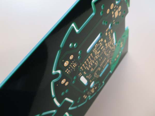
Multilayer PCB |
|
|
|
|
|
I. The components of multilayer PCB: copper foil
A multilayer board consists of copper foils, thin rigid laminates and prepreg sheets. |
|
|
|
|
|
The standard thicknesses for copper foils are shown below
д╠m
|
5 |
9 |
12 |
17.5 |
35 |
70 |
oz |
0.14 |
0.25 |
0.34 |
0.5 |
1 |
2 |
|
|
|
|
|
|
Thick copper (heavy copper) foils are used for voltage and ground planes by some electronics companies. Thicknesses up to 210 д╠m (6 oz) are specified for high voltage coil boards. For very fine-line boards, 5 and 9 д╠m (0.14 and 0.25 oz.), ultrathin copper foils are also used for the outer layers. |
|
|
|
|
|
Copper foils are used as copper cladding of the thin laminates used in the inner layers. Such laminates can be delivered with different copper thicknesses on the two sides, for example, 17.5 д╠m (0.5 oz.) on one side for a signal layer and 35 д╠m (1 oz.) on the other side for ground or voltage planes. |
|
|
|
|
|
Copper foils are sometimes used directly as cap foils for the outer layers. In such cases, the copper foils are bonded to the next layers by means of prepreg and form the outer layer circuits. |
|
|
|
|
|
For signal outer layers, the copper foil thickness is usually 17.5 д╠m (0.5 oz.) or 35 д╠m (1 oz.) depending on the minimum track width and spacing. In the case of high-density fine-line boards, 5 or 9 д╠m (0.14 or 0.25 oz.) ultrathin copper foils can be the only solution to achieve the required high resolution when etching the board. |
|
|
|
|
|
For signal inner layers, a 35 д╠m (1 oz.) copper foil is normally chosen. For ground and voltage planes, 35 д╠m (1 oz.) and 70 д╠m (2 oz.) copper foils can be used. However, the thicker foil, the more difficult it is to fill the apertures in the planes around the hole wall with epoxy flowing from the prepreg sheets during lamination. |
|
|
|
|
|
|
|
|
|
|
|
II. The components of multilayer PCB: thin laminates
Thin laminates are used for inner cores and are available in so many different thicknesses that almost any specified build-up can be accomplished. |
|
|
|
|
|
Different thickness of thin laminates
mm
|
mils |
АА |
mm |
mils |
0.051 |
2 |
0.356 |
14 |
0.076 |
3 |
0.406 |
16 |
0.102 |
4 |
0.457 |
18 |
0.127 |
5 |
0.508 |
20 |
0.152 |
6 |
0.559 |
22 |
0.175 |
7 |
0.610 |
24 |
0.200 |
8 |
0.660 |
26 |
0.250 |
10 |
0.710 |
28 |
0.300 |
12 |
0.760 |
30 |
|
|
|
|
|
|
The thicknesses are valid for the bare laminate, with the copper foil being excluded. We can see the cores are quite thin.? For a total thickness of 1.6mm (0.063inch) board, the more layers, the thinner the laminates should be. See our reference Multilayer PCB stackup for 0.063inch thick. |
|
|
|
|
|
| |
 |
| |
| |
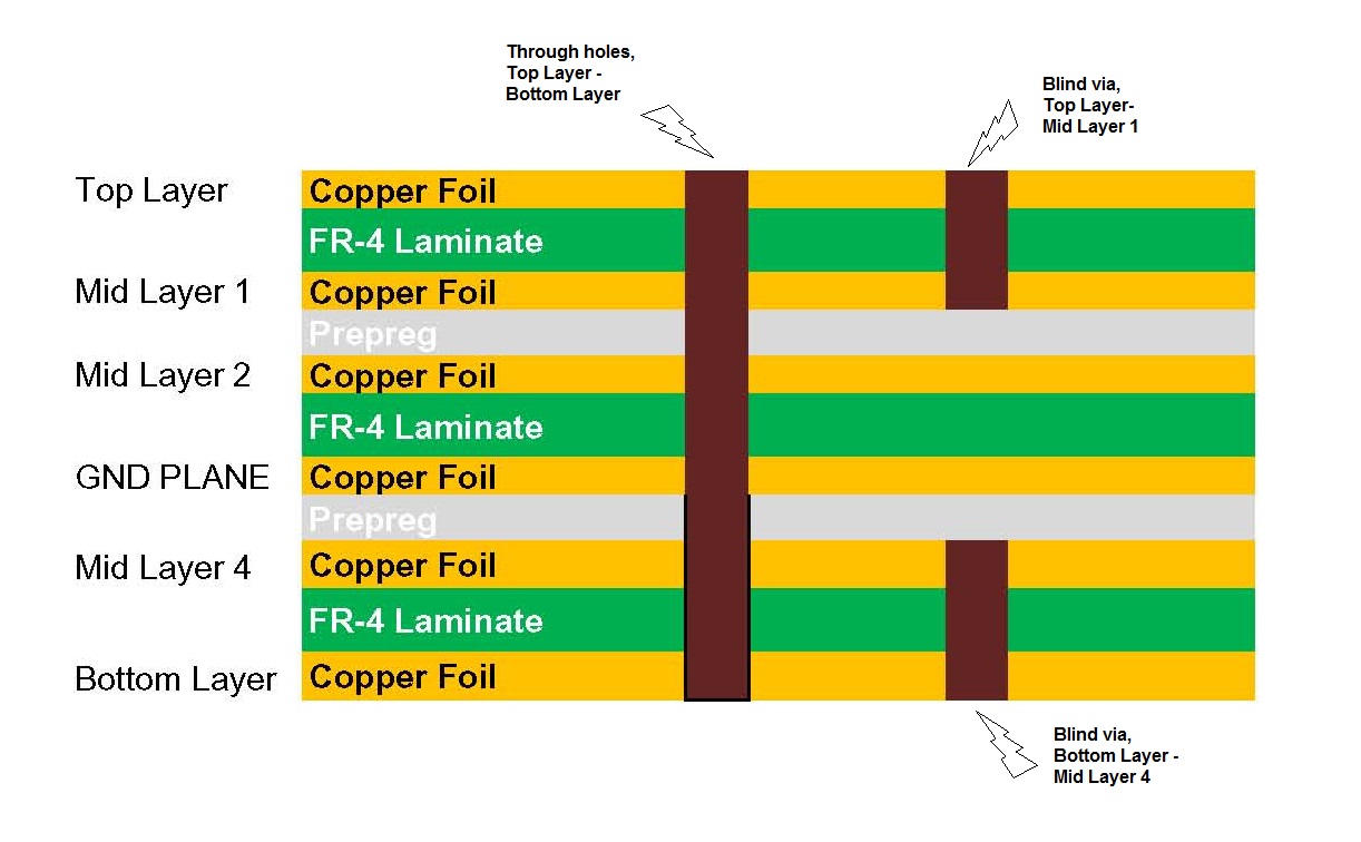
Structure of Multilayer PCB |
|
|
|
|
|
|
|
III. The components of multilayer PCB: Prepreg
Prepreg plays a role of bonding material used for bonding the individual thin laminates of the multilayer boards. It consists of glass cloth impregnated with epoxy resin. Unlike rigid laminates, the epoxy resin is only semi-cured. Epoxy resin is referred to as B-stage when semi-cured. |
|
|
|
|
|
The prepreg sheets are not sticky. During lamination of the board, the epoxy resin is first changed to a liquid state and later in the press cycle to the fully cured state. During the press cycle, the cured epoxy resin in the thin, rigid laminates softens, but it does not become liquid. |
|
|
|
|
|
Thicknesses of Prepreg sheets
Glass Fabric Style
|
Pressed Thickness |
Resin Content |
АА |
mm |
mil |
% |
7628HБе7630БЕ |
0.213 |
8.4 |
50 |
7628Бе43%БЕ |
0.195 |
7.6 |
43 |
7628Бе41%БЕ |
0.185 |
7.3 |
41 |
2116HR |
0.135 |
5.3 |
57 |
2116 |
0.119 |
4.7 |
52 |
2113 |
0.102 |
4 |
56 |
1080 |
0.076 |
3 |
64 |
1060 |
0.051 |
2 |
71 |
|
|
|
|
|
|
The pressed thickness varies from one manufacturer to another. As long as the PCB designer does not know the brand(s) of the glass fabrics used by the multilayer board manufacturer, it is more or less impossible to specify a detailed build-up. Therefore, this should be left to the manufacturer.
When a board is required impedance control, the thickness of the dielectric material between the individual layers become important and thickness and tolerance are usually specified by designer. |
|
|
|
|
|
The minimum thickness of the dielectric material (thin laminate or prepreg sheets) is 75 д╠m (3 mils) and, in some cases, 100 д╠m (4 mils). |
|
|
|
|
|
|
|
|
|
|
|
|
|
|
|
|
|
|
|