|
|
|
|
F4BTME High Frequency PCB
|
|
|
|
|
|
Introduction |
|
|
|
|
|
This series laminates are made by scientifically formulating fiberglass cloth, nano-ceramic filling, and polytetrafluoroethylene resin, followed by strict pressing processes. The series is based on the F4BM dielectric layer, with the addition of high dielectric and low loss nano-level ceramics, resulting in higher dielectric constant, improved heat resistance, lower thermal expansion coefficient, higher insulation resistance, and better thermal conductivity, while maintaining low loss characteristics. |
|
|
|
|
|
F4BTM and F4BTME share the same dielectric layer but use different copper foils: F4BTM is paired with ED copper foil, suitable for applications without PIM requirements, while F4BTME is paired with reverse-treated (RTF) copper foil, offering excellent PIM performance, more precise line control, and lower conductor loss. |
|
|
|
|
|
Features & Benefits |
|
|
|
|
|
- DK range from 2.98 to 3.5 is available - Addition of ceramics enhances the performance. - F4BTME exhibits excellent PIM performance, - Comes in various thicknesses and sizes, offers cost savings - Commercialization, large-scale production, and high cost-effectiveness. - Radiation-resistant and low out-gassing properties |
|
|
|
|
|
Models & Data Sheet |
|
|
|
|
|
Let's go through the data sheet items one by one: |
|
|
|
|
|
Product Technical Parameters and Product Models & Data Sheet: These sections provide an overview of the product's technical parameters and refer to specific models and corresponding data sheets. |
|
|
|
|
|
Dielectric Constant (Typical): This parameter represents the dielectric constant of the material at a frequency of 10GHz. The values for different models are as follows: F4BTME298: 2.98 F4BTME300: 3.0 F4BTME320: 3.2 F4BTME350: 3.5 |
|
|
|
|
|
Dielectric Constant Tolerance: This parameter indicates the tolerance range for the dielectric constant. The values for different models are as follows: F4BTME298: ¡À0.06 F4BTME300: ¡À0.06 F4BTME320: ¡À0.06 F4BTME350: ¡À0.07 |
|
|
|
|
|
Loss Tangent (Typical): Loss tangent refers to the dissipation of energy in the material and is measured at different frequencies. The values for different frequencies and models are provided: At 10GHz: F4BTME298: 0.0018 F4BTME300: 0.0018 F4BTME320: 0.0020 F4BTME350: 0.0025 At 20GHz: F4BTME298: 0.0023 F4BTME300: 0.0023 F4BTME320: 0.0026 F4BTME350: 0.0035 |
|
|
|
|
|
Dielectric Constant Temperature Coefficient: This parameter indicates how the dielectric constant changes with temperature within a specified range. The temperature range is from -55oC to 150oC. The values for different models are as follows: F4BTME298: -78 ppm/oC F4BTME300: -75 ppm/oC F4BTME320: -75 ppm/oC F4BTME350: -60 ppm/oC |
|
|
|
|
|
Peel Strength: Peel strength refers to the strength of adhesion between layers of the material. The values provided are for two different variants: 1 OZ F4BTM: Greater than 1.6 N/mm 1 OZ F4BTME: Greater than 1.4 N/mm |
|
|
|
|
|
Volume Resistivity: Volume resistivity indicates the resistance to the flow of electrical current through the material. The values are given for the standard condition and are greater than or equal to 1¡Á10^7 M¦¸.cm. |
|
|
|
|
|
Surface Resistivity: Surface resistivity represents the resistance to the flow of electrical current across the surface of the material. The values are given for the standard condition and are greater than or equal to 1¡Á10^6 M¦¸. |
|
|
|
|
|
Electrical Strength (Z direction): Electrical strength measures the ability of the material to withstand electrical stress. The values provided are for a test condition of 5KW and 500V/s and are greater than 26 KV/mm for all models. |
|
|
|
|
|
Breakdown Voltage (XY direction): Breakdown voltage refers to the voltage at which the material experiences electrical breakdown in the XY direction. The values provided are for a test condition of 5KW and 500V/s and are greater than 34 KV for all models. |
|
|
|
|
|
Coefficient of Thermal Expansion: This parameter indicates how the material expands or contracts with changes in temperature. The values are given for both the XY direction and the Z direction over a temperature range of -55oC to 288oC. |
|
|
|
|
|
Thermal Stress: Thermal stress represents the ability of the material to withstand temperature-induced stress. The values indicate that there is no delamination when exposed to a temperature of 260oC for 10 seconds, repeated three times. |
|
|
|
|
|
Water Absorption: Water absorption indicates the extent to which the material absorbs water under specific conditions. The values provided are less than or equal to 0.05% when measured at 20¡À2oC for 24 hours. |
|
|
|
|
|
Density: Density refers to the mass per unit volume of the material at room temperature. The values provided are 2.25 g/cm3 for F4BTME298 and F4BTME300, and 2.20 g/cm3 for F4BTME320 and F4BTME350. |
|
|
|
|
|
Long-Term Operating Temperature: This parameter specifies the temperature range within which the material can operate effectively over an extended period. The range mentioned is from -55oC to +260oC. |
|
|
|
|
|
Thermal Conductivity (Z direction): Thermal conductivity measures the material's ability to conduct heat in the Z direction. The values provided are 0.42 W/(M.K) for F4BTME298 and F4BTME300, and 0.50 W/(M.K) for F4BTME320 and 0.54 W/(M.K) for F4BTME350. |
|
|
|
|
|
PIM (Passive Intermodulation): PIM refers to the generation of unwanted signals caused by nonlinearities in the material. The values provided are applicable only to F4BTME and are less than or equal to -160 dBc. |
|
|
|
|
|
Flammability: Flammability indicates the material's resistance to burning. The material composition meets the UL-94 V-0 standard. |
|
|
|
|
|
Material Composition: This section provides information about the components that make up the material. The composition includes PTFE (Polytetrafluoroethylene), Fiberglass Cloth, and nano-ceramics. F4BTM is paired with ED (Electro-Deposited) copper foil, while F4BTME is paired with reverse-treated (RTF) copper foil. |
|
|
|
|
|
| |
Product Technical Parameters |
Product Models & Data Sheet |
Product Features |
Test Conditions |
Unit |
F4BTME298 |
F4BTME300 |
F4BTME320 |
F4BTME350 |
Dielectric Constant (Typical) |
10GHz |
/ |
2.98 |
3.0 |
3.2 |
3.5 |
Dielectric Constant Tolerance |
/ |
/ |
±0.06 |
±0.06 |
±0.06 |
±0.07 |
Loss Tangent (Typical) |
10GHz |
/ |
0.0018 |
0.0018 |
0.0020 |
0.0025 |
20GHz |
/ |
0.0023 |
0.0023 |
0.0026 |
0.0035 |
Dielectric Constant Temperature Coefficient |
-55 º~150ºC |
PPM/¡æ |
-78 |
-75 |
-75 |
-60 |
Peel Strength |
1 OZ F4BTM |
N/mm |
>1.6 |
>1.6 |
>1.6 |
>1.6 |
1 OZ F4BTME |
N/mm |
>1.4 |
>1.4 |
>1.4 |
>1.4 |
Volume Resistivity |
Standard Condition |
MΩ.cm |
¡Ư1¡Á10^7 |
¡Ư1¡Á10^7 |
¡Ư1¡Á10^7 |
¡Ư1¡Á10^7 |
Surface Resistivity |
Standard Condition |
MΩ |
¡Ư1¡Á10^6 |
¡Ư1¡Á10^6 |
¡Ư1¡Á10^6 |
¡Ư1¡Á10^6 |
Electrical Strength (Z direction) |
5KW£¬500V/s |
KV/mm |
>26 |
>30 |
>32 |
>32 |
Breakdown Voltage (XY direction) |
5KW£¬500V/s |
KV |
>34 |
>35 |
>40 |
>40 |
Coefficientof Thermal Expansion |
XY direction |
-55 º~288ºC |
ppm/ºC |
15£¬16 |
15£¬16 |
13£¬15 |
10£¬12 |
Z direction |
-55 º~288ºC |
ppm/ºC |
78 |
72 |
58 |
51 |
Thermal Stress |
260¡æ, 10s£¬3 times |
No delamination |
No delamination |
No delamination |
No delamination |
Water Absorption |
20±2¡æ, 24 hours |
% |
¡Ü0.05 |
¡Ü0.05 |
¡Ü0.05 |
¡Ü0.05 |
Density |
Room Temperature |
g/cm3 |
2.25 |
2.25 |
2.20 |
2.20 |
Long-Term Operating Temperature |
High-Low Temperature Chamber |
¡æ |
-55¡«+260 |
-55¡«+260 |
-55¡«+260 |
-55¡«+260 |
Thermal Conductivity |
Z direction |
W/(M.K) |
0.42 |
0.42 |
0.50 |
0.54 |
PIM |
Only applicable to F4BTME |
dBc |
¡Ü-160 |
¡Ü-160 |
¡Ü-160 |
¡Ü-160 |
Flammability |
/ |
UL-94 |
V-0 |
V-0 |
V-0 |
V-0 |
Material Composition |
/ |
/ |
PTFE, Fiberglass Cloth, nano-ceramics
F4BTM paired with ED copper foil, F4BTME paired with reverse-treated (RTF) copper foil. |
|
|
|
|
|
|
|
Our PCB Capability (F4BTME) |
|
|
|
|
|
Our manufacturing capability includes the following: |
|
|
|
|
|
Layer Count: We are capable of producing Single Sided, Double Sided PCBs, as well as Multilayer PCBs and Hybrid PCBs. |
|
|
|
|
|
Copper Weight: We can accommodate various copper weights for the PCBs, including 0.5oz (17 ¦̀m), 1oz (35¦̀m), and 2oz (70¦̀m). |
|
|
|
|
|
Dielectric Thickness (or Overall Thickness): Our manufacturing process supports a range of dielectric thicknesses or overall thicknesses for the PCBs, including options such as 0.25mm, 0.508mm, 0.762mm, 0.8mm, 1.0mm, 1.016mm, 1.27mm, 1.524mm, 2.0mm, 3.0mm, 4.0mm, 5.0mm, 6.0mm, 8.0mm, 10.0mm, and 12.0mm. |
|
|
|
|
|
PCB Size: The maximum size for PCBs that we can manufacture is up to 400mm X 500mm. |
|
|
|
|
|
Solder Mask: We offer a variety of solder mask colors for your PCBs, including Green, Black, Blue, Yellow, Red, and more. |
|
|
|
|
|
Surface Finish: Our surface finish options are diverse, and they include Bare copper, HASL (Hot Air Solder Leveling), ENIG (Electroless Nickel Immersion Gold), Immersion Silver, Immersion Tin, OSP (Organic Solderability Preservative), Pure Gold, ENEPIG (Electroless Nickel Electroless Palladium Immersion Gold), and other finishes as well. |
|
|
|
|
|
| |
PCB Capability (F4BTME) |
PCB Material: |
PTFE / glass fiber cloth / Nano-ceramic filler |
Designation (F4BTME) |
F4BTME |
DK (10GHz) |
DF (10 GHz) |
F4BTME298 |
2.98±0.06 |
0.0018 |
F4BTME300 |
3.0±0.06 |
0.0018 |
F4BTME320 |
3.2±0.06 |
0.0020 |
F4BTME350 |
3.5±0.07 |
0.0025 |
Layer count: |
Single Sided, Double Sided PCB, Multilayer PCB, Hybrid PCB |
Copper weight: |
0.5oz (17 µm), 1oz (35µm), 2oz (70µm) |
Dielectric thickness (or overall thickness) |
0.25mm, 0.508mm, 0.762mm, 0.8mm, 1.0mm, 1.016mm, 1.27mm, 1.524mm, 2.0mm, 3.0mm, 4.0mm, 5.0mm, 6.0mm, 8.0mm, 10.0mm, 12.0mm |
PCB size: |
¡Ü400mm X 500mm |
Solder mask: |
Green, Black, Blue, Yellow, Red etc. |
Surface finish: |
Bare copper, HASL, ENIG, Immersion silver, Immersion tin, OSP, Pure gold, ENEPIG etc.. |
|
|
|
|
|
|
|
F4BTME PCB and Applications |
|
|
|
|
|
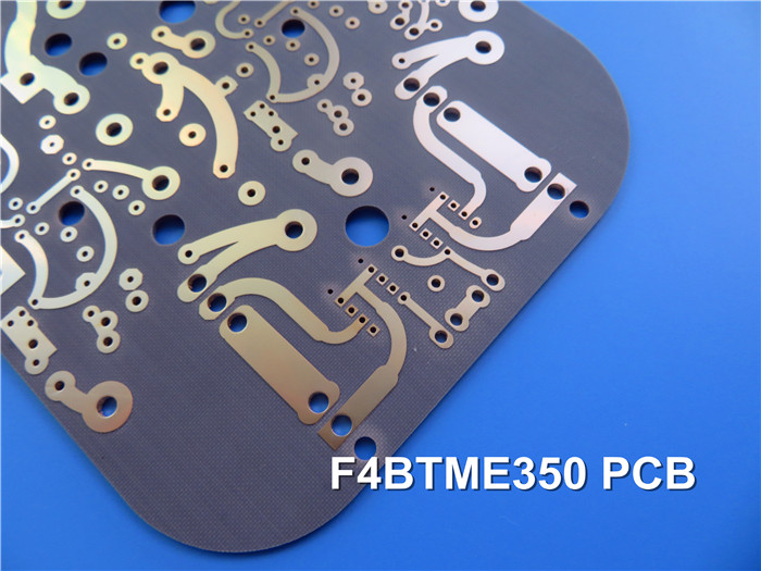
On the screen, you can see a DK 3.5 F4BTME PCB with a substrate thickness of 1.524mm. It has immersion gold surface finishes and 3oz copper tracks. |
|
|
|
|
|
F4BTME series PCBs are employed in a wide range of applications, such as Antenna, Mobile Internet, Sensor Network, Radar, Millimeter Wave Radar, Aerospace, Satellite Navigation, Beidou, Missile-borne, Power Amplifier, and Radio Frequency. |
|
|
|
|
|
|
|
|
|
|
|
Final £¨F4BTME series aluminum-based/copper-based substrates£© F4BTME series of laminates can provide aluminum-based or copper-based materials, where one side of the dielectric layer is covered with copper foil, and the other side of the dielectric layer is covered with either aluminum-based or copper-based material. This arrangement serves the purpose of shielding or heat dissipation. |
|
|
|
|
|
For examples, F4BTME350-CU represents F4BTME350 series with copper-based substrate. |
|
|
|
|
|
|
|