|
|
|
|
|
|
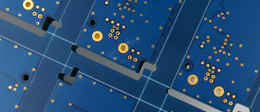
Through hole, Blind via and buried via |
|
|
|
|
|
We can generally see three kinds of PCB via holes and they are respectively through hole, blind via and buried via. |
|
|
|
|
|
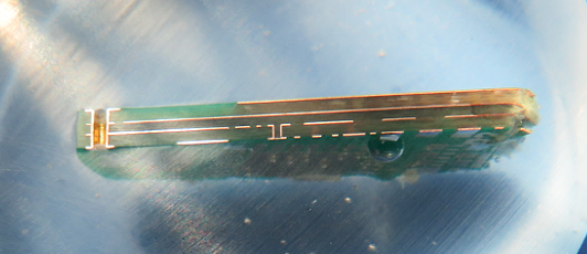
Plated through hole which is also called PTH for short, this is the most common one, if only you take PCB up to the light, the hole in which the light can be seen is "plated through hole". This is also the simplest kind of hole, because it can be done only by using a drilling bit or laser to directly make a full drill in the circuit board at the time of production, and the cost is relatively cheap. But relatively, these plated through holes do not need to be connected for some circuit layers, for example, we have a house of six stories, I bought the third and fourth floor of it, I want to design a staircase in the internal to connect only the third and fourth floor, for me, more space of the fourth floor is invisibly used by the originally connection of the first to the sixth floor. Therefore, sometimes more PCB space will be used even the plated through hole is cheap. |
|
|
|
|
|
|
|
|
|
|
|
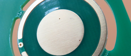
Blind via, the outermost circuit layer is connected with the adjacent inner layer with an electroplated hole, which is called "blind via" because the opposite side cannot be seen. In order to increase the space utilization of PCB circuit layer, the manufacture procedure of "blind via" emerges correspondingly. Special attention is required to be paid to a proper drilling depth (Z axis) for this production method, but this method often results in difficult electroplating in the holes so almost no manufacturers adopt it; You can also drill holes in advance in the circuit layer which needed to be connected at the time of fabricating individual circuit layer before lamination, but relative precise positioning and alignment devices are required. |
|
|
|
|
|
|
|
|
|
|
|
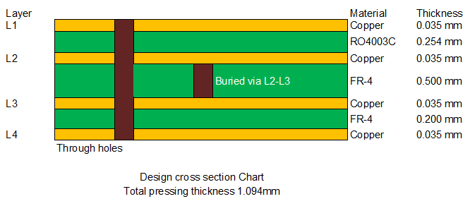
Buried via, the connection of any circuit layers inside the PCB but which is not connected to the outer layer. This manufacture procedure cannot be achieved by means of lamination before drilling. Drilling must be performed at the time of fabricating individual circuit layers. After partial lamination, the inner layer has to be first electroplated before it can be fully laminated. It is more time-consuming compared with the original "plated through hole" and "Blind via hole", so its price is the most expensive. This manufacture procedure is usually only used for high density interconnect (HDI) circuit boards that is to increase the available space of other circuit layers. |
|
|
|
|
|
|
|
|
|
|
|
|
|
|
|
|
|
|
|
|
|
|
|
|
|
|
|
|
|
|
|
|
|
|
|
|